This thread has been locked.

If you have a related question, please click the "Ask a related question" button in the top right corner. The newly created question will be automatically linked to this question.

DAC5652AEVM: Output voltage swing too low

Part Number: DAC5652AEVM

Hello,

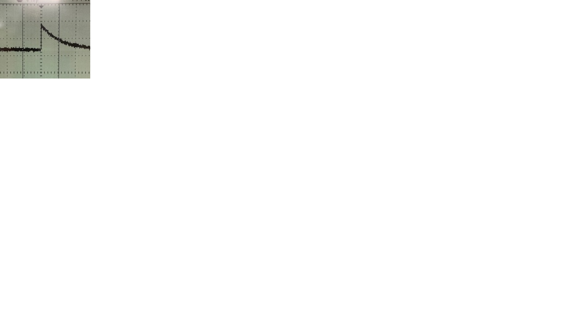
I'm working with the DAC5652AEVM and I have it generating a voltage ramp, but I am seeing a much lower voltage swing than what the datasheet / user guide says I should be seeing. I am using the default configuration for the clock and REXT resistors (2Kohm). Here are the changes I've made to the output as per recommendations by other posts on here:

1. Removed T1 (because the transformer was blocking my low frequency signal)

2. Populated R2 and R28 with 0ohm resistors to bypass the transformer. 

3. Removed R3

4. Changed R4 and R5 to 25ohm resistors (this is shown in the datasheet).

With a 25 ohm load, I'm supposed to see a 1Vpp but I'm seeing close to around 50mVpp. If I change the load resistor R4 to 250ohm, I see the swing improve to around 500mVpp. 

I've checked the EXTIO pin and I'm seeing the correct reference voltage of 1.2V and have verified that the REXT resistor on BIASJ_A is 2Kohms. What am I missing here? Why the discrepancy between what I should be getting and what I'm seeing?

Thanks,
Aditya

  • Aditya,

    You did not follow the data sheet properly when setting up your board for single-ended output operation. Change R5 to 25 Ohms with R4 at 50 Ohms.

    Are you using an oscilloscope to verify the output? If so, make sure it is setup for 50 Ohm loading.  How are the jumpers on J10 configured? Did you verify all digital bits are toggling at the DAC input?

    Regards,

    Jim 

  • Jim,

    I was trying various resistor values. Today, I setup R4 with 50ohms and R5 with 25ohms. I have verified that the data is getting to the DAC along with the clock (using a DLA). I'm seeing a voltage ramp as programmed but at the wrong level as I've said before. The ramp's shape does reflect what I'm doing with the data input. For example, if I make the data change in bigger steps, I see a stepped ramp etc. 

    I am indeed using an oscilloscope to monitor the output voltage. My oscilloscope doesn't allow a 50ohm loading on the input so I had to make one at the o-scope input by using a T junction with a 50-ohm terminator on one side. It is showing a Vpp of 30mV. 

    - Aditya

  • Aditya,

    If you did not modify the second channel, can you generate a sinewave test pattern around 10MHz and verify the board is working with your setup for a sanity check? The BW of the transformer is 800KHz to 200MHz.

    Regards,

    Jim

  • Jim, 

    The best I could do with the equipment I have is to generate a 2MHz triangle wave. I applied this to Channel B and it shows up on the output but I'm seeing the same peak to peak voltage (about 30mVpp with the 50ohm setup, or about 60mVpp without) when looking at the output at J4. 

    I haven't modified Channel B at all. 

    J10 has MODE and GSET set to 3.3V and SLEEP is set to GND. I've tried without any jumpers here but according to the datasheet, these are the default values anyway (MODE and GSET have pullups and SLEEP has a pulldown). 

    I'm powering the evaluation board from a single 3.3V supply. I've shorted JP4 so both J13 and J11 are shorted to 3.3V. When I power the board, it draws about 8mA. The clock source is 0-3V square wave as prescribed by the EVM user guide. 

    I'm not really sure what to change at this point. As far as I can see, I'm doing what I am supposed to. 

    - Aditya

  • Aditya,

    I think you have an issue either with the data coming in or your scope. On channel B, can you try to apply a square wave to the MSB going to the DAC? After going through the transformer, the output should look like what is shown below. What are you using to send the data to the DAC? Is this 0 to 3V level signals? What is the frequency of the clock? The DAC EVM should draw around 100mA. With the DAC EVM powered up, remove your clock source and see if the current changes. Do the same test with the input data.

    Regards,

    Jim

  • Jim,

    I am now pulsing D9 at 10MHz and this is what I see on the output:

    As for the current, I'm sorry. I misspoke. I said 8mA. It was 80mA. So it draws 80mA with the clock applied. If I remove the clock, it draws about 70mA. If I remove the data input, the current draw is unchanged. 

    I am using one of these to provide the digital data inputs: https://store.digilentinc.com/digital-discovery-portable-usb-logic-analyzer-and-digital-pattern-generator/ -- they are 3.3V outputs

    The clock I am providing using a signal generator. I set the output to a 50MHz 0-3V square wave.

    Sincerely,

    Aditya

  • Aditya,

    Your picture did not get attached for some reason. How is the clock source and the data generator synchronized? Can you verify the jumpers are installed as shown in the following table:

    W1

    W2

    W9

    J11

    J11

    J11

    Installed

    Installed

    Removed

    Pins 2 and 3

    Pins 4 and 5

    Pins 10 and 11


    Regards,

    Jim

  • I've uploaded the image here: https://imgur.com/a/YjIKsgY

    The clock and the data source aren't synchronized right now. But here is what they look like. 

    My board doesn't have W1, W2 and W9. J11 is the 3.3V power input. J10 is the one with jumpers. And J10 does have jumpers in those positions.

    Looking at the schematic for this board though, things are a little weird. I didn't notice this until now but the schematic shows DB13->DB0 connected from the part but DB13 is actually DB9 on the package that's on the board. And there isn't a DB13 anyway on a 10-bit part. Not really sure why the documentation is like this (the EVAL user guide actually says connect to pin 55 for DB9 -- which is wrong if you look at the schematic + the actual package pinouts). So if I apply the 10MHZ square wave data input to DB13 (which is really DB9), I get a ~500mVpp peak to peak square wave. Is that what I should be getting? I'm still not getting 1Vpp as the eval states I should but it's closer. Is there something I could be doing wrong for the 500mVpp vs 1Vpp? Is that a loading issue (this is on Channel 2 -- which I have not modified at all).

    Thanks for the help so far, I feel like I'm getting close!

    - Aditya

  • Sorry, reading https://www.ti.com/lit/ds/symlink/dac5652a.pdf again and Page 20 says for the 1:1 transformer, the expected output is indeed 500mVpp. So at least the board is working like it's supposed to besides the schematic / docs issue. 

    On Page 21, they have a single ended circuit that I will likely need for my application and I can't generate the 1Vpp signal as they suggest but that could be because of my 50ohm loading setup I am assuming.

    EDIT: This is just me being an idiot and forgetting I was only flipping D9 from our previous tests. When I flip all bits, I get that full range. 

    Thanks again for your help and patience. I wish I had double checked the pinouts from the EVAL schematic vs the datasheet earlier in this process... 

    Sincerely,

    Aditya

  • Aditya,

    Glad to hear you got this figured out.

    Regards,

    Jim