This thread has been locked.

If you have a related question, please click the "Ask a related question" button in the top right corner. The newly created question will be automatically linked to this question.

DDC264EVM: Data acquisiton format issue in 16Bit Mode

Part Number: DDC264EVM
Other Parts Discussed in Thread: DDC264

Dear colleague,

The customer wants to use DDC264EVM to compare their DDC264 data acquisition result.

But when they use DDC264EVM in 16bit, they encounter below issues.

They want to know:

1. What is the reason for the wrong output format in the 16bits configuration?

2. In output summary, the value is averaged by GUI, how many times have an average? How to get the row data? Because they want to compare their DDC264 data acquisition result with DDC264EVM, now they this their board noise is large.

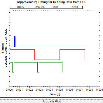
When change format to 16bit, no matter input signal amplitude and frequency how to change, output in GUI is wrong, and max value is not 65535. Result is as below:

When change format to 20bits, output changed with input signal changes, the result is normal. The result is as below:

Connection configuration:

  • Hello Rock,

    There is a bug in the FPGA firmware in 16-bit mode.

    A fixed value of 16711680 in decimal (0xFF0000) needs to be subtracted from the data.

    The Single Channel Line Plot in the Graph tab presents the sequential series of data for a single channel.

    This will show the number of samples taken into consideration for the average.

  • Hi Praveen,

    According to your suggestion, the customer has got the raw data. But now they have concerns about the difference between A and B channel.

    The customer test process:

    1. Replace the channel 128,94,35 resister by PD in DDC264EVM. The common end is connected to ground.

    2. Place EVM in a shielded environment (without any light and isolate electromagnetic radiation interference)

    3. Set different gain(11-00 total are 4 kinds of gain), integrated time is 1000us and 2500us. Get raw data in 20bit and 16bit.

    Result as below:

    Standard deviation is standard deviation of 512 samples.

    The customer concerns are:

    1. In 00 gain, the difference between A and B are very large as marked by red box. Is it right?

    2. Whether the standard deviation is normal?

    Thanks a lot!

    Best Regards,

    Rock Su

  • Hi Rock,

    If we look at the boxes you squared in red, the difference scales with range as one would expect it to be if it was due to charge (more on that below). I.e., between range 3 (150pC) and range 0 (12.5pC):
    1. Range 0: 5812-2899=2913
    2. Range 3: 4108-3848=260 --> one would expect this to be x150/12.5=3120 in Range 0.

    So, to me sounds about right. I.e., any charge error at the input that was creating 260 codes on range 3 will produce more than 10x bigger error at the 12.5pC scale. The number does not exactly match as offset is not all due to a charge at the input but also through other constant factor (that would not scale with range) but it is super close...(for lack of a more scientific term :))

    Now, one would wonder what is the source of that charge to begin with. A potential mechanism for this offset is that the input bias voltage of the amplifier of the A side (Va) is slightly different than the B side (Vb). When A is disconnected, that input bias voltage gets sampled in the Cdet (sensor and trace parasitic capacitance) and that charge gets transferred to the B side when this is connected if the input bias voltage of B is not exactly the same as A. Notice that the bigger the Cdet the bigger the charge that gets transferred. 3000 counts at 12.5pC would be 35fC. This would correspond to Cdet x (Va-Vb).

    This is just a theory, so, can they confirm that the difference becomes much smaller if they use test mode (disconnect the input) or simply unplug the PD (photodiode)? Do they know the capacitance value of the parasitic of their PD?

    So, in conclusion, the offset mismatch between A and B side looks right and can be removed through standard calibration/subtraction. Nevertheless, one thing that looks maybe too big is the noise. They seem to be talking about 50ppm of FSR in Range 3, isn't it? Looking at the DDC264 DS, we see that to get that level of noise one would need 1000 pF PD (bottom right of the table) which is quite big.

    Can they confirm that their PD is really that big? If not, can they look at the noise number again without PD or better, in test mode? And how about the noise value for any other input? Usually noise increases due to lack of shielding, for instance, so, it would also be visible in other inputs with no PD. Is the shielding box grounded?

    Regards,

    Edu

  • Dear Eduardo,


     Thank you for your understanding and help, under your guidance and encouragement, we have carried out the test.


    According to the last feedback, there are three main points:

    1. After replacing the photoelectric array on the development board, the static offset measurement value meets the expectation and the error is acceptable, and the source of the error may be the lack of scientific measurement method and device;
    2. PD detector capacitance may be too large, resulting in excessive noise. Is it determined as 1000pF?
    3. Change register to test mode and observe the noise level at the moment, or do not change to test mode and force the analog current end to ground and observe the noise change.


    The test results of the last two of the above three points are as follows:

    1. Combined with the feedback information, the experiment was conducted with an integral time of 5000us and a gain of 00. Firstly, register bit0 was set to 1 to test the mode. At this time, the two-channel noise value was read near 8.8 PPM, as shown in Figure 1. Follow the manual description. The data points read normally and the fluctuation is as expected.


    Figure 1


    2. Set the register bit0 to 0, at the same time simulate the PD current end null connection, the connector suspension processing, read the noise at the moment at 5000+ PPM, the reason is unknown. Data point anomalies, fluctuations deviated from expectations.


    1. Next, keep bit0=0 and ground the voltage input end of the analog current plate, equivalent to no signal input. Read the noise at the moment at 7000+ PPM, for unknown reasons.


    According to the above test conditions:

    Q1What are the possible reasons for the above problems?

    Q2The PPM difference between DDC264 chip A and chip B in the test mode is about 2‰. In non-test mode, it is about 2% without detector. In non-test mode, it is about 8% when connected with detectoris it normal for the difference to be so large?


    About the capacitance of PD detector:

    For the stray capacitance of PD detector, digital bridge test is adopted. 100KHZ frequency, parallel mode, measuring capacitance of bridge, the capacitance value of PD was separately tested near 57pF, the line capacitance was below 5pF, and the DDC264 input capacitance was separately tested near 6pF. DDC264+ wiring +PD=70pF nearby. The last measurement of 1000pF was due to the use of series mode and 1KHZthis time the use of parallel mode for large impedance devices can improve the accuracy.

    Table 1


    The last question is that the integrator A and B can be calibrated according to your introduction. Do you have any recommendation on the calibration method?

    Thanks again for your patience.

    Best Regards

    Lynn Li

  • Hi Lynn,

    Thank you very much for your detailed explanations and experiments.

    Just to clarify the first initial 3 conclusions:

    1/ I am not sure what you mean for "the source of the error may be the lack of scientific measurement method and device;" but basically I was meaning that the offset difference between A and B is expected to increase as the range becomes smaller (gain becomes bigger). Bottom line, the offset difference look ok.

    2/ Yes, to get that large noise of 50ppm at Range 3, the input parasitic should be about 1000pF. I agree that this is likely not the case and believe much more the 70pF so one should be measuring about 8ppm rms in Range 3 (not 50 like the first post indicated). So, something is wrong here...

    3/ Test mode disconnects the input from the external world. The alternative is to leave the device in normal operation and leave the input floating, not connected to ground. The input is a current input (not voltage), hence to avoid having any current at the input, one has to leave the input disconnected/open. So, this would explain why your 3rd experiment "keep bit0=0 and ground the voltage input end of the analog current plate" gave you such large values. 

    Nevertheless, it is not clear on the first two experiments:

    1. On the first one, you seem to be in 20b mode, isn't it? In principle that should not make a difference as you are reporting ppm but just looking for some software bug... As you are in TM I expect this noise to be very small, but I am surprised is only ~9ppm of 12.5pC. It is even below the 0pF of the spec table, but I agree that with TM you are even below 0pF as you are disconnecting also some of the input capacitance inside the IC. So, it could be... Only strange thing is that your average is around 150 and not closer to 4095. Maybe I am missing something in the software (will ask folks here).
    2. The 2nd one I really don't understand. What do you mean for "simulate the PD current end null connection". Is this equivalent to the experiment you originally reported? I.e, PD connected but not illuminated? In this case, in the original measurement, you had about 500 ppm of noise in range 00 (12.5pC), but now it is 5000 so, I'm really missing something. Also, the samples seem to be jumping from -2000 to 2000? By the way, you picked a different channel (256A vs 253A in the previous experiment). Is that right?

    On the calibration question, the simplest way is to measure few k points, maybe 4096, for each side, A and B, with no signal (PD connected but no illumination/x-ray off), average those samples (separately for A and B) and obtain two value DCA and DCB. Then you can subtract from now on DCA and DCB from the data that comes from A and B. 

    By the way, let's see if the above helps solve your questions, but if the posts become too slow we can also jump into a call. We can take this thread off-line...

    Regards,
    Edu

  • Dear Eduardo,

    Thanks for your reply,I'd like to trouble you again!

    We also found some problem in the test results through your reply last time. We boldly speculated that it might be the EVM. Therefore, we obtained another EVM and tried to test again. The specific process is as follows (using the new ddc264 EVM);          

    1. The assessment board is short circuited by jumping cap, as shown in Figure 1;           

    Figure 1  

       2. On this basis, start the software and connect the evaluation board, as shown in Figure 2;        


    Figure 2            Set the configuration register, integration time 2500us, 20bit, gain 00, chip for C series;          

      3. After the configuration is successful, data acquisition is performed, as shown in Figure 3-4;     


    Figure 3           

    256a channel, PPM data range from - 5 * 103 to 15 * 103           


    Figure 4  The noise of a integrator is 6876, and that of B integrator is 7479;           

    Through the test, it is found that whether the first EVM or the second EVM test, the data obtained are very different from the EVM datasheet. However, we always believe that the measured data of ddc264 should not be the data obtained by us, but should be the data from the EVM datasheet.  we are eager to ask you to help us analyze whether there are problems in our testing methods  at Present, which lead to errors in obtaining data. Can you provide relevant tutorials or help you infer the possible causes of data errors Thank you for your help. Looking foward to recieving from you.

    Best Regards

    Lynn Li

  • Hi Lynn,

    That's a good way to start. Just get from the EVM the DS result... (which of course is not the graph that you show, as you imagined).

    Settings/timing looks like it should work. What do you mean for "is short circuited by jumping cap"? Are you saying that you put a cap between the input of channel 256 and the ground? That would be ok. Short circuiting the input to ground would not be ok, as explained...In fact, the easiest test you can do is to unplug the AIB (Analog Interface Board), the small board... Another thing you can do is to set bit zero to "1", i.e., enter test mode, which will disconnect the input and remove some of the concerns above.

    Another thing, whenever you work with external connection (not in test mode), is to put the setup in a shielded box. Notice that the inputs in range zero are extremely sensitive. 30ppm of 12.5pC is 0.37fC! So, the device will pick up any small signal coupling at the inputs, specially if you have something like in the picture, with the AIB not connected to anything/floating. In that sense, from the shape of the signal plot, it looks to me that you have some kind of envelop (not just random noise). You are sampling every 2.5ms and the China grid frequency is 20ms (50Hz). The figure shows only the A samples, so, samples every 5ms. If I am looking at this right, you can actually see how the samples ran on a 50Hz signal... For instance, starts on top, then you get one half way, then the one that hits the bottom, clipping, then another half way, then one on top, and so on:

    So, if I had to bet, this is it... 50Hz coupling to your inputs. Test mode will make everything look good. Shielded box will solve the problem too.

    Regards,
    Edu 

    Note: Looking at the figure respect to the settings, did you click update plot? It doesn't seem to match but I'll ask someone else more familiar with the software to take a look... Regardless, I don't think it affects the result. It is just a display thing.

    1. CONV: 2.5ms (12500 / 5MHz) --> This doesn't look right (the CONV is not low for 2.5ms)
    2. CLK = 5MHz --> DVALID about 276us (you can see that in the figure from CONV edge to falling edge of DVALID)
    3. DCLK wait = 13k / 80MHz = 0.16ms (from the falling edge to DVALID to the beginning of the blue packet of data out)
    4. DCLK: 40MHz --> Readout time: 256*20*25ns=0.13ms about the width of the blue band/rising edge of DVALID)

  • Hi Lynn,

    The timing plot below is what you should see if you use the "Update Plot" button. However, it shouldn't affect the settings or the data capture. Thanks.

    Regards,

    TC

  • Dear Eduardo,

          Thanks for your help, we have got the result with your help. As expected, the reason why the data obtained is inconsistent with the manual is mainly due to the test environment. Through the evaluation of the measured data of EVM and the minimum gain in the manual, under 20bit, 320us integration time, the collected data noise has more than ten ADC values, which are different from the 6.5adc value proposed in your manual (we understand it as the difference between the test and the environment). The two internal A / b integrators do have different differences under different gains, as shown in Table 1 below;   


     The minimum gain / integration time is 320us, the noise is about 16.4, and there are 10 ADC value differences compared with manual 6.5; the internal A / b integrator has a difference of 0.7% in bias value and 0.4% in noise difference, but the gain is the largest. The difference in bias value of internal a / b integrator is increased to 3.1%, and the noise difference is increased by 10.6%. With the increase of integration time, the difference in bias value of internal A / b integrator is increased to 40%, and the noise difference is 10.5% Please also help to analyze from a professional point of view, whether the above obtained data, especially the difference value of a / b integrator, is true and credible (can we understand that there is a difference in a / b integrator, and this difference is consistent with our above test results, maybe you can directly help to give the difference of a / b integrator, thank you!) In addition, we will continue to test downward based on the above test results. Please help us evaluate whether the test method is reasonable? Thank you for your support!   The above data are all tested in static state (static definition: ddc264 input terminal is connected with GND through 10m resistance, without signal access). In the future, we will collect stable data of ddc264 and evaluate the chip noise and integrator difference under open state condition (open state definition: ddc264 input terminal is connected with photodetector, and the detector is placed in a fixed light intensity environment, equivalent and stable) Input) test the response value and noise of ddc264 chip          

     The test steps are as follows:            

    1. Replace the input connection resistance of ddc264 chip of EVM with PD. PD is a 16 point photodetector, and PD diode cathode is connected to GND. The connection is shown in the figure below;     

       2. PD is implanted in the stable light intensity environment, and the output signal of ddc264 chip is collected by setting different gain and different integration time;         

       3. The overall response value and response noise of ddc264 chip after accessing PD are evaluated by collecting data signals.


    Bset  Regards

    Lynn Li

  • Hi Lynn,

    Let me try to study the data a bit but I'll reply to some of the questions on my next post. 

    In the meantime, can you please upload the table with higher resolution? I may be able to figure it out but it is quite hard to read...

    Thank you!

    Edu

  • Hi Lynn,

    I tried making sense of the table with the help of your explanation... If I get it right, first row is noise and third is offset code (that you call "bias value"). What are the other rows? Let's see if I can address your questions here:

    "The minimum gain / integration time is 320us, the noise is about 16.4, and there are 10 ADC value differences compared with manual 6.5; the internal A / b integrator has a difference of 0.7% in bias value and 0.4% in noise difference, but the gain is the largest [I think you meant 0.2% and for the lowest gain, largest range]. The difference in bias value of internal a / b integrator is increased to 3.1%, and the noise difference is increased by 10.6%. With the increase of integration time, the difference in bias value of internal A / b integrator is increased to 40%, and the noise difference is 10.5% "

    Have you checked repeatability of your measurements? I.e, are these results always the same? As you said, the environment noise seems to be quite large so it could distort the results... The only way for me to check it is to look at the 20b and 16b data, and percents do not seem the same. I assume you took the data with different DDC setting (so, at different times) but mathematically, if it was repeatable, changing from 20b to 16b probably would not change anything on the percentages, while in the data you show, it does.

    Also, just one note on the analysis, regardless if the measurements are right or wrong... You seem to try to quantify things in percent... But to do so, you probably need to consider that offset is the error respect to the output for zero input, which is not zero, but 4096. Therefore, A bias would be 3964.8-4096=131 and B bias would be 4433.6-4096=337. The gain difference between the two ranges is 12.5pC to 150pC, i.e., a factor of 12. On the lower gain you got about 10 codes difference (3838 to 3847) so, one would expect about 120 codes at the higher gain but you got 337-131 = 206. So, a bit higher... Again, I would first make sure that the results are repeatable.

    When you move to the longer integration times, couple of things can happen. First, I am not sure how is that affecting the sampling of the interferers but as fundamentally both A and B sides are being taken at the same time just shifted by one sample, it is the difference on that one sample in time that will make the final difference. I would think that longer integration makes this difference more likely bigger. Regardless of that, as you increase the integration time, the offset mismatch may increase too. The reason is not offset by itself, but the fact that any input current (ibias) mismatch will show up (its effect will be more significant) as you increase the integration time. With shorter integration times, the ibias effect may be negligible respect to the offset, for instance. 

    In general, if you want to have a baseline, I would recommend measuring things in test mode, with the inputs disconnected. That should remove interferers from the equation and give you an overall sense of what you should be expecting, best case. 

    I do not know about analyzing things with a "fixed light intensity". We do not have such sources in the lab here and I don't know drift or noise associated to them. Drift for a mismatch analysis should be ok, I would think, though. One trick to check if something is coupling from outside (or for instance, the light source is noisy) is that all the channels/PD should see the same problem at the same time. So, while adding all channels together, in the time domain, sample by sample, should effectively reduce the peak to peak, if the light source has some kind of noise this will show in all the channels at the same time and hence it will not average out across channels but increase linearly with the number of channels and become obvious.

    Regards,
    Edu

  • Dear Edu,

    Sorry to reply you so late.We are also adding some tests and data processing. Originally, we planned to complete the supplementary test and provide the supplementary test results before replying to you, but the results were not as expected. We provide you with the attached data sheet of the above questions. Please check it. In addition, as mentioned above, we are conducting the supplementary test. After the test results come out, we can also communicate. Thank you for your special support!

    Best Regards

    Lynn Li

  • Dear Edu,

    Sorry to reply you so late, mainly because we are also adding some tests and data processing. Originally, we planned to complete the supplementary test and provide the supplementary test results before replying to you, but the results were not as expected. We provide you with the attached data sheet of the above questions. Please check it. In addition, as mentioned above, we are conducting the supplementary test. After the test results come out, we can also communicate. Thank you for your special support!

    Lynn Li

  • Hi Lynn,

    Thanks a lot for going through the effort of reformatting the table/data.

    I am not sure I recall. When you say EVM, do you mean our board or your board? And does your data show that actually when you plug your detector to the board the noise goes down? Maybe that is acting as shielding... (?) Are you putting everything in a shielded box?

    Anyhow, will wait for your further results :)

    Best regards,
    Edu