This thread has been locked.

If you have a related question, please click the "Ask a related question" button in the top right corner. The newly created question will be automatically linked to this question.

ADS8344EVM: How to config Power Supplies Settings and Pins on ADS8344 EVM ?

Part Number: ADS8344EVM
Other Parts Discussed in Thread: ADS8344,

Hello

I'm trying to connect ADS8344 EVM with ATMEGA128.

But I'm not sure how to config for the Power, GND and lots of Fuses.

Please let me know which setting is correct once external +5V DC using .

I tried to set Power Supplies as guide document but EVM doesn't work.

I did connect SS,SCK,MOSI and MISO on P2 and Power Supplies setting as well.

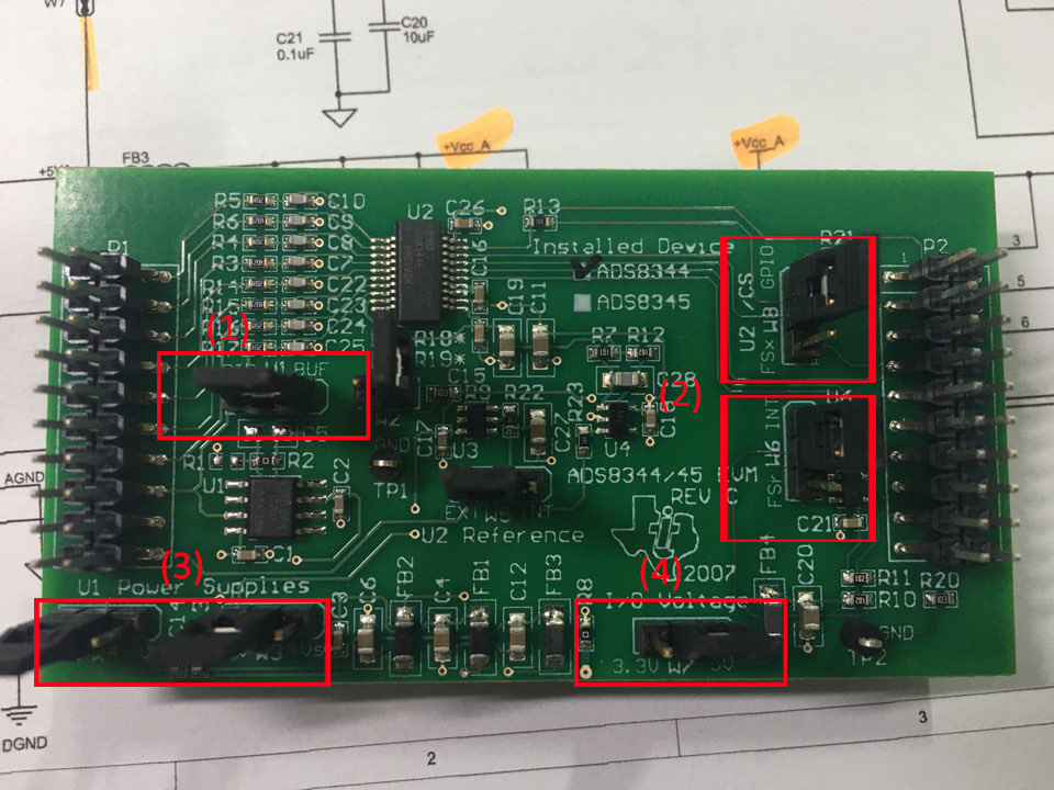
I would like to know for details as below attached picture.

Thanks in advance.

  • Hi Wooseong,

    Welcome to our e2e forum!

    Let's start with box 1 and 3 - you don't really need those to get started with the ADS8344EVM.  They control the power to a buffer amplifier used on CH7.  For the two (2) boxes, W6 and W8 as shown above are in their default locations.  This is shown in the schematic with the black lines tying pin 1 and 2 of the jumper together.  W6 sends the BUSY output of the ADS8344 to pin 15 of P2 - you can tie that to an interrupt pin on your controller.  W8 ties the chip select input to pin 1 of P2 - this is your SS input.  Box (4) shows W7 with a shunt on pins 1-2, which connects your supply voltage to J3 pin 10.  Our controller usually puts 5V there.

    For the second image, showing J3, pin 1 would be in the bottom right hand cornePin 10 is in the upper left hand corner.  So, from right to left as shown above, the bottom row is 1,3,5,7 and 9.  The upper row is 2,4,6,8 and 10.  You must also tie the ground of the ADS8344EVM to your controller board.  There are no fuses on the EVM, those are ferrite beads!

  • Hi Tom.

    I really appreciate your kindly support.

    I'm asking you one last time.

    Could you review settings as below ? If those settings are correct or not.

    P1 :  pin1(SS), pin3(SCK), pin11(MOSI), pin3(MISO)

    P2 : pin2~pin6(Input voltage)

    W1 W2 W3 W4 W5 W6 W7  W8 

    pin1,2

    (Jumper)

    OPEN

    pin1,2

    (Jumper)

    pin1,2

    (Jumper)

    pin1,2

    (Jumper)

    pin1,2

    (Jumper)

    pin1,2

    (Jumper)

    pin1,2

    (Jumper)

    J3 : Pin5,6(GND), pin3(input +5VD), pin10(input +5VD)

    BRs

    W.S.

  • Hi Tom.

    Finally, I did resolve issue about this case.
    Thanks for your great help.

    I found HW problem on EVM I have.There are some floating point so it didn't work till now.
    It works well after fixed floating point and I can test ADC value for each channel.

    I did set HW settings as below.
    -------------------------------------------------------------------------
    P1
     :  pin1(SS), pin3(SCK), pin11(MOSI), pin3(MISO)
    P2 : pin2~pin6(Input voltage)

    W1 W2 W3 W4 W5 W6 W7  W8 

    pin1,2

    (Jumper)

    OPEN

    pin1,2

    (Jumper)

    pin1,2

    (Jumper)

    pin1,2

    (Jumper)

    pin1,2

    (Jumper)

    pin1,2

    (Jumper)

    pin1,2

    (Jumper)

    J3 : Pin5,6(GND), pin3(input +5VD)pin10(input +5VD)
    -------------------------------------------------------------------------

    BRs
    W.S