This thread has been locked.

If you have a related question, please click the "Ask a related question" button in the top right corner. The newly created question will be automatically linked to this question.

ADS114S08: Getting full scale reading when reading data from ADS114S08

Part Number: ADS114S08
Other Parts Discussed in Thread: ADS114S06,

Dear Sir,

We are back to this project once again.

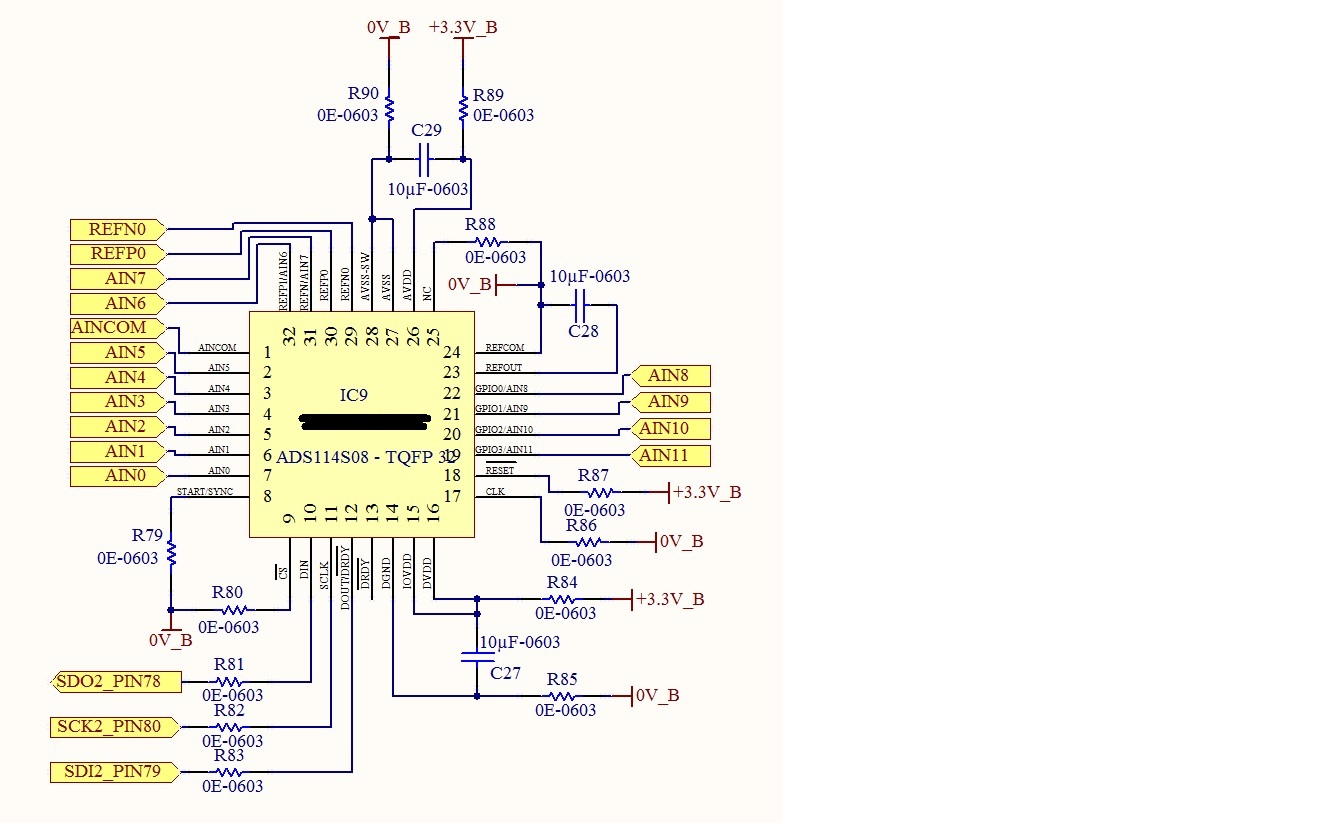
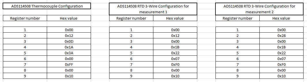
Previously we are using IC ADS114S06.

But now our channel requirements are change so we are now change IC as ADS114S08.

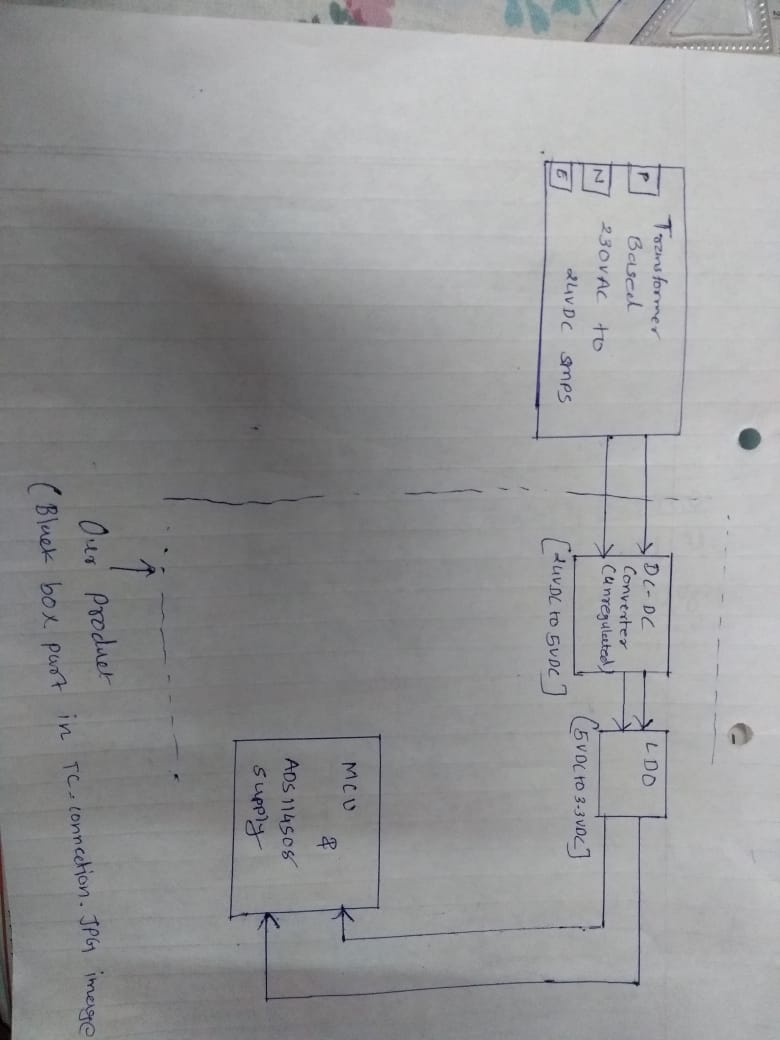
Here below I have attached updated schematic diagram of circuit.

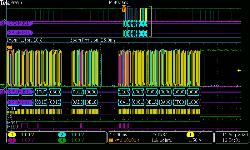
Consider all 3 controller pin (SDO,SDI,SCLK) connections are proper and directly connected to MCU.

There are no any external Pull UP / Pull Down resistors connected.

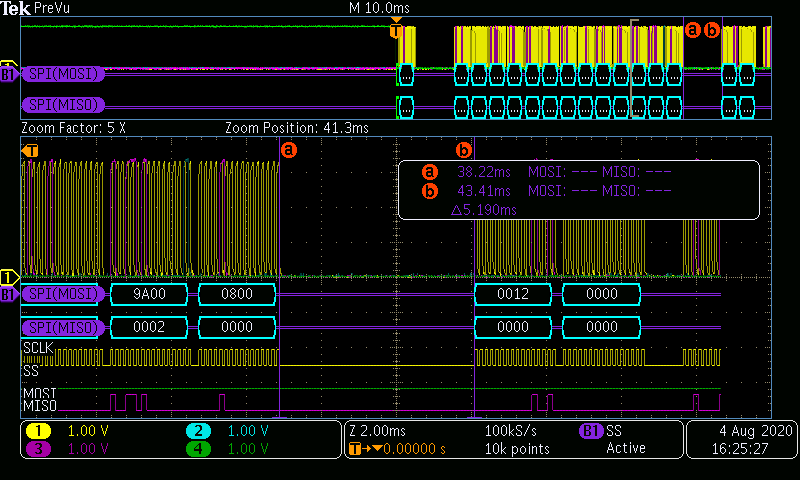
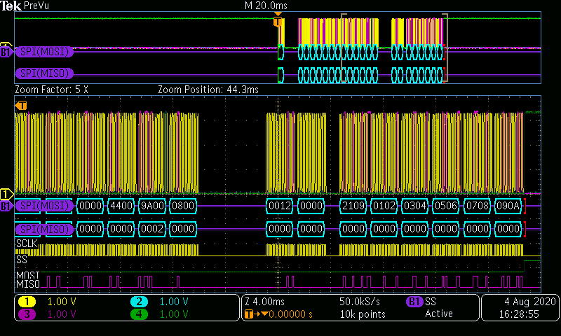
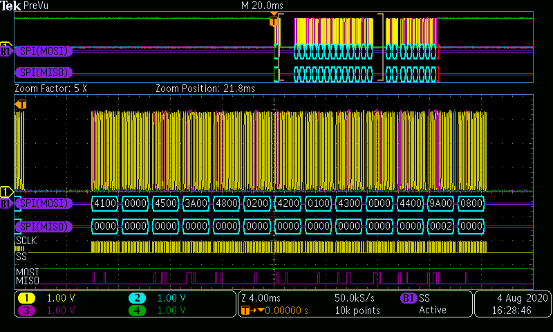
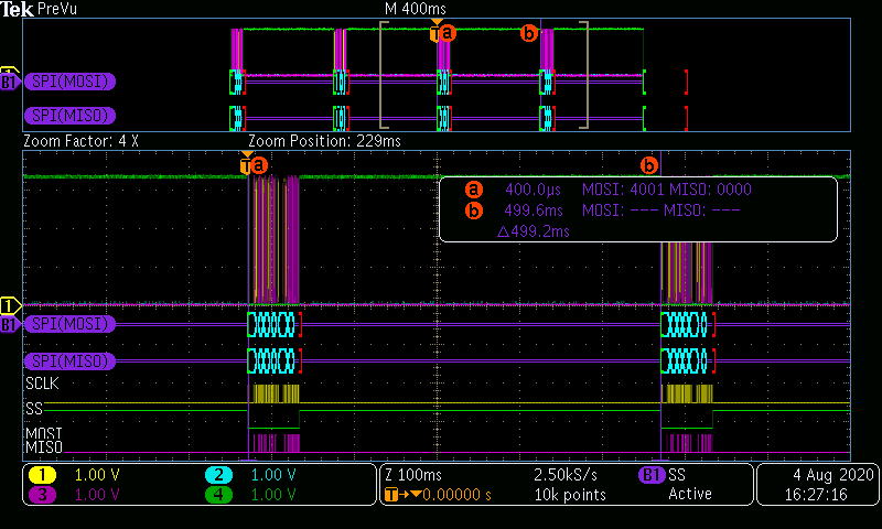
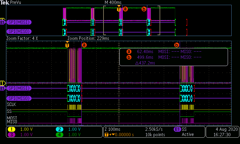
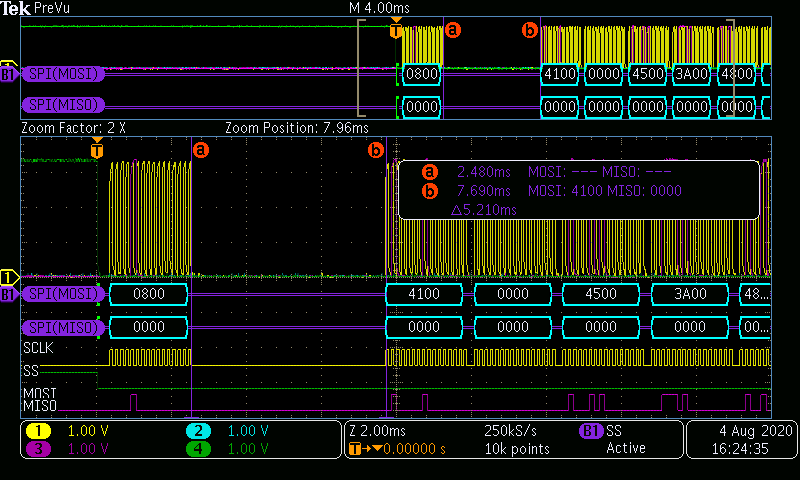
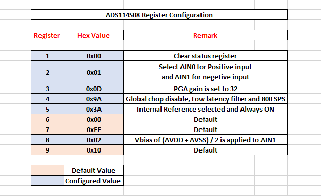
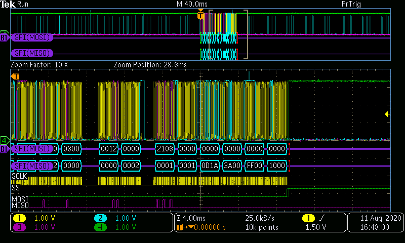
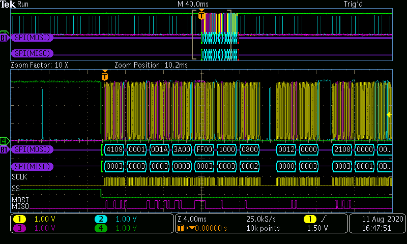
Currently we are trying to read ambient temperature of IC (system register value 0x50, Reference register value 0x1A, PGA value 0x09)

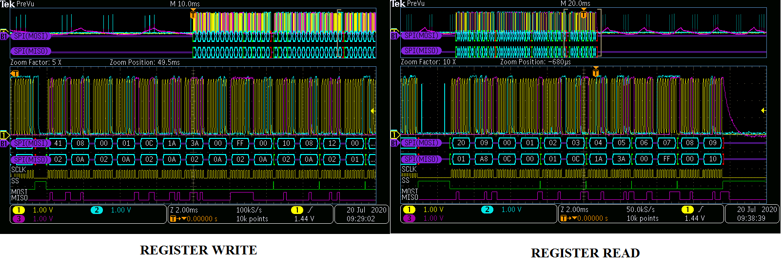
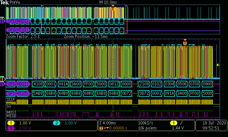
But we are always getting full scale reading (0x7FFF) instead of desired results.

Please suggest us proper solution for same.

Let us know is there any hardware modification is required or not?

Waiting for your quick reply.

Thanks and best regards,

Jehan Patel

  • Hi Jehan,

    I'm not sure what you mean by "There are no any external Pull UP / Pull Down resistors connected".  You cannot leave digital inputs float, so they must be properly connected to the appropriate levels.  For one example, the RESET pin must be pulled high or the device could float and enter a reset state.  The CLK pin must be set low, or the ADS114S08 could stop operating.  Can you give me more detail as to your schematic and how the pins are truly connected?

    Have you verified that the registers were written correctly by reading back the contents?  Have you monitored the analog supply to make sure that it is operating at nominal operating voltage?  Have you check the voltage or REFOUT to make sure that it is operating at 2.5V?

    Best regards,

    Bob B

  • Hi Bob B,

    Thanks for your reply.

    First as you said all digital inputs must connected to appropriate level, we do the same and connected digital input pins to appropriate level.

    (RESET pin is pulled high , CLK pin is pulled low with this START and CS pins are also pulled low)

    Second you suggested to check on REFOUT and REFCOM pin, we are getting 2.4630V though 1uF capacitor. its like charging and discharging not constant voltage we getting.

    All supply are as per mention in datasheet. 

    After all this modification in our circuit we trying to read default values of registers,  but we are getting random values for all register  and after some time all register become zero so tell us what is problem.

    Let us know is there any hardware modification is required or not?

    Waiting for your quick reply.

    Thanks and best regards,

    Jehan Patel

  • Hi Jehan,

    This sounds like you are using a prototyping system that may have long wires interconnecting various supplies and control lines.  If you are seeing the REFOUT with a charge/discharge cycle then it would appear that the supply is drooping either because of current limiting or perhaps poor grounding.  I would look into the reference output connections as well as the analog and digital supply connections.

    Best regards,

    Bob B

  • Hi Bob B,

    First if all thanks for your reply.

    As per your suggestion we reduced interconnecting wires length, now we are getting  constant 2.4946V at REFOUT. 

    But now we facing problem with RESET, we have connected RESET to 3.3V to use RESET command (0x06) but still ADS114S08 reset on Power On RESET.

    Waiting for your quick reply.

    Thanks and best regards,

    Jehan Patel

  • Hi Bob B,

    with previous reply i want to add that whenever we give RESET command (0x06) ,we did not get default data. To get default data we have to manually toggle RESET pin. So give us proper RESET pin connection for hardware.

    Waiting for your quick reply.

    Thanks and best regards,

    Jehan Patel

  • Hi Jehan,

    The ADS114S08 will reset when power is applied to the device (both analog and digital) after the supplies have reached nominal operating voltage.  Toggling the RESET pin will also issue a device reset as will issuing the RESET command.  If the RESET command is not resetting the ADS114S08 you should monitor the communication with an oscilloscope or logic analyzer.  Noise on the SCLK or DIN can result in the command being ignored. 

    As you are holding CS low, it is quite possible that noise has affected the communication with little ability to regain communication without the hardware RESET on the pin.  There is an SPI timeout feature to help with these issues when CS in permanently tied low (toggling CS resets the SPI communication).  The default setting for the timeout is disabled but can be enabled in the SYS register (9h), but you have to have valid communication prior to setting this bit.  The SPI timeout when enabled will reset the SPI bus following the timeout period.

    I think you still have some wiring issues that is affecting your communication.  Perhaps running at a slower SCLK rate would help during prototyping.

    Best regards,

    Bob B

  • Hi Bob B,

    As per your suggestion we observe SCLK and DIN on oscilloscope and below is image of that. we observe spike on SCLK and DIN. We also observe spike on DIN when nothing is transferred to ADS114S08. 

    with this i want to add that first we are sending 8-bit  data for configuration of ADS114S08 that does not work and after that we changed it to 16-bit  data for configuration of ADS114S08 which works fine. So we want clarify that is there any difference if we configure ADS114S08 with 8-bit or 16-bit data. Because in datasheet they clarify it.

    Thanks and best regards,

    Jehan Patel

  • Hi Jehan,

    It appears that you are picking up significant noise on the communication wiring.  Noise on SCLK will be very problematic as this will cause an extra clock causing an issue with decoding of the command within the ADS114S08.

    The communication is byte oriented for the ADS114S08.  You can send multiples of a byte (such as 16 bits) without issue, but it is unclear as to what you mean by sending 8 bit data for communication that does not work.  Can you send me scope shots of each type of communication so that I can compare to see what may be different?  Unless you are now using CS on the device instead of holding it low.  If you attempt to use the SS pin on the SPI peripheral this will be an issue as the communication must hold CS low on the ADS114S08 for the entire communication transaction.  The SS pin would toggle in 8-bit mode every byte which would then cancel the communication.  It is better to control the CS pin with a GPIO instead of the peripheral for cases where more than 2 bytes are sent such as when using the RDATA command.

    Best regards,

    Bob B

  • Hi Bob B,

    1) After Implementing all your suggestions we reading analog signal(1mV) from channel 0 and 1 by setting gain of 16 and Data rate of  4000 SPS (0x0E in Register 4).we are getting desired reading through RDATA (0x12) command but after sometime result goes to zero and again it goes to our desired reading. during this REFOUT is contant 2.4975V. So what is cause for this zero reading...

    2) after that we set gain of 32 and Data rate of 20 SPS  for that we getting zero reading for same analog signal (1mV) .

    3) sometime after writing into registers and read them back for verification we getting zero value for all configured registers.

    Thanks and best regards,

    Jehan Patel

  • Hi Jehan,

    I think you are actually spending more time debugging your prototyping situation than actual verifying a design.  It is pretty obvious to me that the route of all your issues is the way you are trying to do this.  There is a reason for PCBs and why systems are not built with a bunch of fly wires.  So you need to improve your prototype so that there is proper power and ground connections, clean with no spikes communication, and that any noise or physical contact with the prototype is prevented.

    See additional responses below.

    Best regards,

    Bob B

    Jehan Patel said:

    Hi Bob B,

    1) After Implementing all your suggestions we reading analog signal(1mV) from channel 0 and 1 by setting gain of 16 and Data rate of  4000 SPS (0x0E in Register 4).we are getting desired reading through RDATA (0x12) command but after sometime result goes to zero and again it goes to our desired reading. during this REFOUT is contant 2.4975V. So what is cause for this zero reading... [Bob] This appears to be corrupted communication where the RDATA command is not properly decoded.

    2) after that we set gain of 32 and Data rate of 20 SPS  for that we getting zero reading for same analog signal (1mV) . [Bob] Have you verified that the registers are written as expected, including the mux input settings?  If the device has reset, then you also need to make sure that you issue the START command or that the START pin is pulled high.

    3) sometime after writing into registers and read them back for verification we getting zero value for all configured registers.[Bob] This appears to be due to a reset condition that has taken place.  This could be caused by a poor connection with either power or ground in the IOVDD, DVDD or AVDD pins.

    Thanks and best regards,

    Jehan Patel

  • Hi Bob B,

    thanks for your quick reply and all suggestions.

    1)  Here is image of configuration of ADS114S08 via 8-bit data and 16-bit data. first image is for 8-bit and second for 16-bit data transmission. as there any difference  if we use 8-bit or 16-bit.

    Here is link (http://ww1.microchip.com/downloads/en/DeviceDoc/70005185a.pdf) for SPI configuration we have used. Go to page-8 SPI Control register 1, in that MODE16 bit 1 or 0 create problem or not. We have used CKP & CKE = 0.

    2) During reading of analog signal from sensor, device earth where sensor mounted create problem or not for measurement.

    Thanks and best regards,

    Jehan Patel

  • Hi Jehan,

    The problem with the byte length communication is where CS goes high.  If CS goes high in the middle of a communication then the command will cancel.  Also, you could potentially have the same kind of issue with 16-bit communication, but it so happens that CS is changing on an appropriate boundary.  Here is what is incorrect with the 8-bit communication:

    Note that I have placed X where CS should not toggle and be held low.  I also added a | where it would be the correct place to toggle CS.  If you are manually controlling the action of CS then you should make sure that it toggles at the correct time.

    Regarding '2', it is quite possible that you could see noise from a ground loop if the sensor earth ground also connects to one of the ADC inputs.

    Best regards,

    Bob B

  • Hi Bob B,

    1) when we didn't connect earth to sensor or device same result appears when we connect earth to sensor or device.

    2) with this i want to add that our desired result is varying its not constant even the analog signal source is constant what is cause for this variation in converted  result.

    Thanks and best regards,

    Jehan Patel

  • Hi Jehan,

    Most likely the noise is being picked up in wiring.  If you use any gain, the noise will be gained up as well.  Common noise sources are power line-cycle noise, RFI and EMI.  EMI is most often due to motor noise and RFI can come from most anything these days including WiFI and cell phones.  Basically it is very difficult to design a precision system with just wiring components together.  It takes a great deal of effort including good PCB layout and even then it can be difficult to achieve low levels of noise.

    Best regards,

    Bob B

  • Dear Bob,

    As you can see, we are not sure for this part performance yet.

    So we have prototype design. Once we got satisfactory desired results for all different thermocouples and RTD sensors. 

    We will definitely move for PCB testing.

    But at current stage we have to complete this prior testing on bread board connection only.

    please check out below points and give me update for same.

    1) As you can see in circuit diagram we made all connections as per the datasheet suggestions.

    We are already getting desired output for ungrounded J type and K type thermocouples.

    But we are getting varying output for grounded J type , grounded K type and exposed tip thermocouples.

    As you already know that major of equipments have earth connection for safety precautions, we already connect earth to our equipment also and it is properly connected.

    Can you please explain us the reason behind the varying output for grounded thermocouples?? We are measuring voltage of grounded thermocouple on DMM and it is steady it is not varying!

    Hope your explanation should not contain only noise level parameters and add other technical things also. Because we measured voltage at AIN0 and AIN1 (Thermocouple input channel) which is always steady and not varying. so it is concluded that it is not noise level issue. 

    2) How does selected part number will affect to the measurement system if the connected sensor is earth or not?

    3) What is the maximum ESD protection on all pin of IC to overcome external high voltage changes?

    Waiting for your quick reply.

    Thanks and Best regards,

    Jehan Patel

  • Hi Jehan,

    As I stated a few posts back, I believe you are not really measuring or analyzing the performance of the ADS114S08 but rather your prototyping solution.  As to your breadboard solution, I don't really know how you have things currently connected as there were issues with your initial implementation and I don't know how this was resolved.

    For 1) Normally when you connect equipment together you would isolate systems so that one system doesn't interfere with the other.  When you have power supplies, micros, etc. connected together you are also creating a ground loop.  This ground loop is caused from powering your system from the power AC distribution.  When you measure with the DMM, you are in a sense isolating the DC measurement from the circuit.  Also, this DMM measurement is not necessarily accurate as there will be some significant averaging within the meter itself that may cancel some noise.  So yes, my explanation does include noise as a varying signal for a DC source is noise.  Where the noise originates and how much of an impact it makes is difficult to fully ascertain as I'm not able to be with you to troubleshoot your design. Perhaps some pictures of your setup and how you have things connected would help.  The ADS114S08 will power from a source and especially where the ground return to the source may be just some wires, there will be a highly inductive path in the ground.  The ADC requires a clean ground (no bounce or ripple) for both the analog supply and the reference.  This will not impact the measurement for the DMM as the measurement is isolated, but will directly impact the measurement by the ADS114S08.

    For 2) A secondary issue with grounding the TC to earth is that the common-mode now shifts and may also be outside of the measurement range of the ADC if the earth ground and the analog ground are at the same potential.  If the system is not an isolated system, then using bipolar analog supplies may be beneficial.  In this case AGND is at mid-supply and well within the common-mode of the PGA.

    For 3) The ESD protection within  the device is specified in the ADS114S08 datasheet in section 7.2 on page 5.  The primary purpose of the ESD protection in the ADS114S08 is for device handling and machine operation when building boards or assemblies.  It is not designed to handle large transients and requires some external mechanism such as Schottky or TVS diodes.  So the system should be designed to protect the ADS114S08 against large transients or over-voltage conditions that may result in the Absolute Maximum Ratings (section 7.1) of the ADS114S08 to be exceeded.

    Best regards,

    Bob B

  • Dear Bob,

    Please checkout below points it may helpful to us for resolving this thread quickly.

    1) We checked all supply voltages on oscilloscope as per below connectio.

    Measurement-1 : Pin-16 (DVDD) and Pin-14 (DGND) voltage.
    Measurement-2 : Pin-26 (AVDD) and Pin-27 (AVSS) Voltage.
    Measurement-3 : Pin-23 (REFOUT) and Pin-24 (REFCOM) Voltage.
    Measurement-4 : Pin-18 (RESET) and Pin-14 (DGND) voltage.

    Here below we have attached zip file which contains all 4 measurement logs for more than 10 min constant observations.
    where we do not found any noise level.

    2) We also checked voltages at 2 different measurement channels.

    Measurement-5 : Pin-7 (AIN0) and Pin-6 (AIN1) measurement channel 1 voltage for grounded J type thermocouple input.
    Measurement-6 : Pin-5 (AIN2) and Pin-4 (AIN3) measurement channel 2 voltage for grounded J type thermocouple input.

    we have set 150 °C DUT temperature and it is steady where thermocouple voltage on true RMS multimeter is 6.58mV and it is steady.
    so as per thermocouple voltage, if we check NIST standard J type LUT temperature value is around 126 °C.
    our CJC temperature value is 30°C so total temperature value is 156 °C approximately.

    DUT body is properly connect to earth so thermocouple body is also connect to earth.

    we have connected channel 1 and channel 2 with J type grounded thermocouple where both have same mV input as mentioned above.

    3) As per the voltage waveforms we can conclude that there are no any connection issue. we are giving constant mV input to ADS channel still we are getting varying values on SPI.

    Can you give us detail description for cause of this problem?

    Waiting for your quick reply.

    Thanks and Best Regards,Voltage Waveform at different Pins of ADS114S08.xlsx
    Jehan Patel

  • Hi Jehan,

    Looking at the data file you sent, the most concerning was the measurement from REFOUT to REFCOM.  The reference appears to be oscillating and this could be due to a poor ground or a missing cap.  The reference should be very stable and if not you will see variations in the output code.  I would concentrate on making sure that the reference output voltage will stay stable and should be within the min/max of the datasheet electrical characteristics.

    Is it possible for you to send a few pictures of your setup so I can verify other potential issues with your setup?

    Thanks,

    Bob B

  • Dear Bob,

    Please check log data properly, reference voltage is constant around 2.5 to 2.6 voltage. 

    Please use data filter concept on excel sheet to see results.

    Time  Voltage (VDC)
    -0.02 2.32
    0.1082 2.48
    0.18 2.44

    Here you can see out of 2500 samples only 3 samples are less than 2.5VDC which is not problematic.

    Regarding missing capacitor concept, we have connected 10uF capacitor where datasheet suggested value for capacitor is1uF to 47uF.

    Please find attached image of thermocouple setup and earth connection give to system. 

    We already checked all connectivity for earth connection it is found to be ok.

    Redarding 3.3VDC and GND supply, We are using isolated regulated 24VDC to 3.3VDC supply so it is not relevant to earth connection any how.

    so all connection are perfect. All voltage value are also ok.

    waiting for your quick reply.

    Thanks and Best Regards 

    Jehan Patel

  • Hi Jehan,

    Please remember that you are very familiar with the data collected and the setup you are using whereas I am not.  In your previous response you stated:

    "1) We checked all supply voltages on oscilloscope as per below connectio.

    Measurement-1 : Pin-16 (DVDD) and Pin-14 (DGND) voltage.
    Measurement-2 : Pin-26 (AVDD) and Pin-27 (AVSS) Voltage.
    Measurement-3 : Pin-23 (REFOUT) and Pin-24 (REFCOM) Voltage.
    Measurement-4 : Pin-18 (RESET) and Pin-14 (DGND) voltage."

    And in the spreadsheet I see values for Measurement-3 that range from:

    Minimum Value (Volt) 2.32
    Maximum Value (Volt) 2.64
    Average Value (Volt) 2.567936

    The internal reference as specified in the ADS114S08 data sheet in the electrical characteristics table provide the following for the TQFP package:

    TA = 25°C, TQFP package: –0.05%(MIN)  ±0.01%(TYP)  0.05%(MAX) , So the initial value will be 2.5V +/- 250uV typical and worst case is 2.5 +/-1.25mV.  So when I see values like 2.32V or 2.64V and even an average value of 2.568 I have great concerns about the stability of the reference.  All I have to go on is the information that you are willing to share and have provided.  At some point I have to make some assumptions which may or may not be valid.

    Thanks for the pictures you did send, but here again I have to make some assumptions as you did not explain the connections.  I assume that the shielded cable that connects to the terminal block is the grounded tip TC, is that correct? And then you show a clip lead but not where the other end connects, so is this the connection to earth ground?  And then there is another wire that connects to the terminal block (center) and what does this wire connect to?

    So I need really detailed information:

    • As to how the inputs are connected from the TC to the ADC inputs (pictures and explanations would help here as well)
    • A detailed schematic with what you are using for antialiasing filters at the inputs
    • Information as to how you are setting the common-mode for the TC
    • All register settings being used
    • Raw data (hex or decimal but hex preferred) but not converted to a voltage value for at least 128 to 256 continuous and contiguous (every completed conversion sample with no conversions being skipped) data conversions

    From your perspective your design is complete, no problems or issues.  But the data results you are giving me point to some issue in your setup.  If the TC before connecting to earth measures ok, but when connecting to earth there is a problem then this points to something either to the device settings or connections to the device.

    As I explained before, if you are using the PGA then the input must be at least within the input range of the PGA.  If the earth ground places the TC connection at the same point as AGND, then you will be outside of the input range of the ADS114S08 with the PGA enabled.

    If you have a long wire connection between the TC and the earth ground, then this wire will be highly inductive and even though from a DC perspective may seem to be stable, the wire itself is highly inductive and susceptible to AC noise pickup the same as an antenna.

    So for me to help you troubleshoot your solution, I need to have much greater detail as to how you are trying to implement the solution.  Diagrams, pictures, complete schematics and detailed explanation along with the raw data will be very helpful.

    Best regards,

    Bob B

  • Dear Bob,

    Please check out below confirmations for more details.

    1)      Shielded cable connected to the thermal block is Grounded J Type Thermocouple

    2)      Connected clip 2nd connection is connected to earth.

    3)      Wire connected to center of the thermal block is another Grounded J type Thermocouple which is connected to control system. So it not relevant to our measurement system anyhow.


    From your query please find other details required to you is as per below.


    1)      “As to how the inputs are connected from the TC to the ADC inputs (pictures and explanations would help here as well)”

    -          Please find attached image TC_Connection.jpeg


    2)      “A detailed schematic with what you are using for antialiasing filters at the inputs”

    -          Please find attached image ADS_RC_NETWORK.jpg


    3)      “Information as to how you are setting the common-mode for the TC”

    -          Sorry but did not get your point. Please explain in detail


    4)      “All register settings being used”

    -          We want to measure thermocouple data for 2 different channels (AIN0-AIN1) and (AIN2-AIN3). Please find attached image Config.JPEG. We have implemented this sequence in SPI code in MCU. And it showing ok on oscilloscope. You can find previously attached images for more details. And as you know CS pin is permanently low so there is no any requirement of CS pin waveform.


    5)      “Raw data (hex or decimal but hex preferred) but not converted to a voltage value for at least 128 to 256 continuous and contiguous (every completed conversion sample with no conversions being skipped) data conversions”

    -          Please find attached excel for more information


    6)      “From your perspective your design is complete, no problems or issues. But the data results you are giving me point to some issue in your setup. If the TC before connecting to earth measures ok, but when connecting to earth there is a problem then this points to something either to the device settings or connections to the device.”

    -          Please take a note if we connect earth to the system or not, we are getting varying results continuously.

    7)      “As I explained before, if you are using the PGA then the input must be at least within the input range of the PGA. If the earth ground places the TC connection at the same point as AGND, then you will be outside of the input range of the ADS114S08 with the PGA enabled.”

    -          As we know J type thermocouple maximum voltage range is 69 mV. For PGA enable and gain value 32 this range is cover in ADS114S08. It is not out of the range value. Also we have measured thermocouple voltage before connect to PCB and it is as per the current temperature of thermal block.


    8)      “If you have a long wire connection between the TC and the earth ground, then this wire will be highly inductive and even though from a DC perspective may seem to be stable, the wire itself is highly inductive and susceptible to AC noise pick up the same as an antenna.”

    -          It is around 1 meter. And in industries it is more than 5 to 10 meters. But as our system earth connection is proper than length does matter anyhow.


    9)      Regarding REFOUT and REFCOM voltage value please find attached video where we got constant 2.5VDC voltage but still we observed varying data from ADS114S08. As we know that these voltages are generated from IC internally and our supply voltages to digital supply pins and analog supply pins are constant still, we don’t know reason for getting varying results on SPI. Please explain in brief for same.

    Hope you have all necessary details for now.

    We can coordinate on call for discussing this issue. We are available in office from 9 AM to 7 PM IST (GMT+5.30)

    Waiting for your quick reply.

    Thanks and Best Regards

    Jehan Patel

    ADS114S08_RDATA Reading.xlsx

  • Hi Jehan,

    Now I think I understand what 'varying' means along with your comments about the result not being related to noise.  Thanks for the video of the reference voltage.  Also thanks for verification of your register settings and the status of CS.

    Regarding number 9, as the meter is showing a steady voltage, what voltage measurement in particular is varying?  Does this specifically relate to the analog inputs of the TC or is there another measurement that is also varying?  

    I think your issue may be a result of one of 3 possible scenarios:

    • Corrupt communication
    • Common-mode input range
    • Loose wiring

    For the moment lets take loose wiring out of the conversation.  The reason I had asked for verification regarding CS is you show CS tied low, but in some of your communication scope shots you sent previously you show CS toggling.  So if you hold CS low permanently there is the possibility of data corruption due to spurious SCLKs.  If this should happen, the data could become corrupted.  To understand your communication further could you explain the following or send code snippets of the communication:

    • How are you determining when to read the conversion results? (For example, are you monitoring DOUT/DRDY, using a timer, etc. And if you are monitoring DOUT/DRDY are you polling the result or using an interrupt driven system to read the result?)
    • Do you read the data direct from the ADS114S08?  Or are you using the RDATA command?
    • Do you have access to a logic analyzer to monitor the signals MISO, MOSI, SCLK during the capturing of data? This would be important for me to see the actual timing of data collection and to determine why and when the data is changing.
    How are you making the measurements?   Are you using a method similar to shown below?
    1. Configuring for measurement 1
    2. Waiting for the result and reading it
    3. Changing the configuration to measurement 2
    4. Waiting for the result and reading it
    5. Repeat back to 1
    • When you change the from measurement 1 to measurement 2, are you just writing the change of the input mux, or are you writing the whole configuration again? (You only need to write the mux input change, and in fact if there is an issue with communication the PGA gain setting may be changing inadvertently where the gain of 32 may be changing to a gain of 2 or 16 which would result in a varying output code. )

    Let's discuss the input range as it relates to point 3 above.  The ADS114S08 has a limited input range as given in the Recommended Operating Conditions in section 7.3.  This is specified relative to AVDD/AVSS and PGA gain.  For a gain of 32 it appears as follows:

    Note that the TC is a floating voltage and relative to the ADC input could float to any value including outside of the analog input range.  If the TC becomes grounded relative to AVSS, note that this is outside of the input range.  There are a couple of ways to position the input within the correct range.  One is to use pull-up and pull-down resistors at the TC input to force the input to be approximately (AVDD-AVSS)/2 which is well within the input range.  Another method would be to use VBIAS which you would turn on for the AINN input to set the floating input voltage at the VBIAS voltage.  These settings are configured in register 8h.  Here you could set the VBIAS configuration to be connected to AIN1 and AIN3.

    Best regards,

    Bob B

  • Hi Bob,

    Please checkout below points and give comments for same.

    1) In previous comment attached video indicated voltage between REFOUT and REFCOM and attached excel have varying results of Channel 1 and Channel 2 measured voltage SPI data reading

    2) "I think your issue may be a result of one of 3 possible scenarios:

    Corrupt communication
    Common-mode input range
    Loose wiring"

    Please note below points

    corrupt communication -- we already sent you communication waveform in previous comments which is found to be ok
    common mode input range -- i think we have set PGA and data rate value in thermocouple input range so it is not useful to us.

    as per datasheet page no.6, for PGA=32 and VINMAX = 70 mV minimum V(AINX) is 1.235VDC and maximum V(AINX) is 2.065VDC.

    Loose wiring -- as you can see attached TC_Connection.jpg image we are working on PCB so loose wiring not possible. We already check thermocouple connection to terminal which is ok.

    3) "For the moment lets take loose wiring out of the conversation. The reason I had asked for verification regarding CS is you show CS tied low, but in some of your communication scope shots you sent previously you show CS toggling.
    So if you hold CS low permanently there is the possibility of data corruption due to spurious SCLKs. If this should happen, the data could become corrupted. To understand your communication further could you explain the following or send code snippets of the communication:"

    In communication waveform CS pin is not used because it is permanently ground as you can see in RC_network.JPG image.
    Our Communication is working ok. Our code sequence in MCU is fix as per below lines

    • Power on MCU
    • Configure SPI in mode with 16 bit communication mode
    • RESET ADS114S08 using Commands
    • Configure ADS114S08 for Internal CJC Measurement
    • START ADC Conversion using START Command
    • Delay of 1 mSec
    • Read CJC data using RDATA command
    • RESET ADS114S08 using commands
    • Configure ADS114S08 for Burn out Detection for channel 1
    • START ADC Conversion using START Command
    • Delay of 2 mSec
    • Check Burn out detection using RDATA command
    • RESET ADS114S08 using commands
    • Configure ADS114S08 for channel 1 measurement
    • START ADC Conversion using START Command
    • Delay of 10 mSec
    • Read Channel 1 measurement using RDATA command
    • RESET ADS114S08 using commands
    • Configure ADS114S08 for Burn out Detection for channel 2
    • START ADC Conversion using START Command
    • Delay of 2 mSec
    • Check Burn out detection using RDATA command
    • RESET ADS114S08 using commands
    • Configure ADS114S08 for channel 2 measurement
    • START ADC Conversion using START Command
    • Delay of 10 mSec
    • Read Channel 2 measurement using RDATA command

    for above whole sequence everything working ok for ungrounded thermocouple. but when we are connecting grounded thermocouple we are getting varying channel measurement data as per last comment excel data.
    which indicated there are no any communication error. So please give us proper suggestions.

    4) "How are you determining when to read the conversion results? (For example, are you monitoring DOUT/DRDY, using a timer, etc. And if you are monitoring DOUT/DRDY are you polling the result or using an interrupt driven system to read the result?)"
    check above code sequence you will get the answer.

    5) "Do you read the data direct from the ADS114S08? Or are you using the RDATA command?"
    we don't know about direct reading data from ADS114S08 so we are using RDATA command only.

    6) "Do you have access to a logic analyzer to monitor the signals MISO, MOSI, SCLK during the capturing of data? This would be important for me to see the actual timing of data collection and to determine why and when the data is changing."
    you can find waveforms on older comments.

    7) "When you change the from measurement 1 to measurement 2, are you just writing the change of the input mux, or are you writing the whole configuration again? (You only need to write the mux input change, and in fact if there is an issue with communication the PGA gain setting may be changing inadvertently where the gain of 32 may be changing to a gain of 2 or 16 which would result in a varying output code. )"
    we are writing the whole configuration again. changing the gain value is not possible because this code sequence working ok for ungrounded thermocouple, CJC measurement, burn out detections!

    8) Please check above code sequence and let us update what is exact delayed required after each configurations. Also let us know that stop command is required or not.

    9) we checked the results by applying 1 Mohm pull up and pull down resistors on Thermocouple +ve input and -ve input respectively. But still we are getting variations in results from 98 °C to 115 °C for thermal block temperature stable at 110 °C. Please suggest us proper pull up and pull down resistors value, we will implement it in our PCB and check results that we got steady results or not.

    Thanks and Best Regards,

    Jehan Patel

  • Hi Jehan,

    I'm sorry that you are having such issues.  We have many countless customers making TC measurements without issue.  There is some mechanism that is not clear as to what is causing the varying result.  A couple of things that only today have I become aware.  The first is the use of the burnout current sources (BCS).  The second is the repeated resetting of the ADS114S08. 

    I think the BCS could be a big part of the problem.  You have a very large time constant filter, and when the BCS are energized it could take 10's of milliseconds for the analog input to settle once the BCS are turned off.  The very first thing I would do is to make this as simple of a process as possible until we can determine why the output code is varying.

    Set up the device by  only taking a single measurement of the grounded TC.  If you can collect long term stable data with only one input, add the second measurement.  Otherwise we need to analyze why that data becomes varying.  Most likely the input is floating to a value outside of the input range.  Yes this can happen and you shouldn't exclude the possibility just because you think the input range is not being violated.  The reason being is the CMOS input can float to either supply rail.  Another thing you could look at is to turn off chopping to see if that improves the measurement.

    Once the first measurement is stable, add a second measurement.  This could either be the 2nd TC measurement or the CJC measurement.  In any case only add one variable at a time.  Do not keep resetting the device between configurations, but rather just change the register settings.  Once you have 2 measurements stable, add the 3rd.

    For the burnout check the better way to conduct this measurement is to not issue the BCS check and then immediately read that same channel for the measurement.  Give the system time to settle following the BCS measurement.  Stagger the burnout check between the 2 TC measurements and CJC measurement.

    The STOP command can be used between measurements but is not necessary.  In your current implementation the RESET will automatically stop the device from converting.

    When you added the 1M pull-up and pull-down resistors, you were still having variation in the results, but it would appear that the variation is much less, is this correct?  Appropriate resistor values would range from 1M to 10M Ohm.  If there was an improvement, do you have data you can share with me?

    Best regards,

    Bob B

  • Hi Bob,

    As you suggested we tried with only one measurement first and with this we also removed reset command.
    so after that our code sequence in MCU is fix as per below lines

    • Power on MCU
    • Configure SPI in mode with 16 bit communication mode
    • Configure ADS114S08 for Internal CJC Measurement
    • START ADC Conversion using START Command
    • Delay of 1 mSec
    • Read CJC data using RDATA command
    • Configure ADS114S08 for Channel 1 (AIN0+ & AIN1-) Measurement
    • Delay of 3 mSec
    • Read Channel 1 data using RDATA command

    This sequence is implemented in 500ms timer ISR.

    we observe that variation in channel 1 input voltage value from 6.048 to 6.921 mV where the thermal block is stable at 150˚C.

    Second as per your suggestion we removed pull-up/pull-down from measurement channel 1 and used internal V bias voltage of (AVDD + AVSS) / 2.
    Note that we applied V bias voltage on AIN1- as you mention in older comments.
    but when we used internal V bias of ADS114S08 we got random data. And after some time all data reset to 0. When this situation occurs we measured voltage between REFOUT and REFCOM and it found to be zero. please explain this condition in brief
    Whenever we apply earth connection to thermocouple sheath at that time all communication reset to zero and measurement voltage between REFOUT and REFCOM is zero.

    Thanks and  Regards,

    Jehan Patel

  • Hi Jehan,

    You didn't exactly follow what I instructed, but at least we know a little more.  I wanted just one measurement and not a sequence of 2 measurements as I wanted to know if switching from the CJ measurement might also cause an issue due to analog settling.  But I think we may have some good clues anyway.  When you turn on VBIAS there is so much current drawn through VBIAS that the ADS114S08 is resetting.  So it would appear that your isolated supply is not so isolated from earth ground.  Discontinue the use of VBIAS and determine what the supply and TC inputs measure relative to earth ground with the voltmeter.  Check first to make sure that the voltage from the supply to earth ground does not exceed the analog supply voltage you are using.  If it does, then you definitely have a supply isolation issue.

    If the analog ground is the same potential as the earth ground with respect to the voltage measurement taken with the voltmeter, then this will also be a problem as the PGA input is then violating the input range.  In the case where the analog ground is the same potential as the earth ground, you will need to disable the PGA and use a gain of 1.  The other alternative is to use bipolar analog supplies (+/-2.5V) where ground is mid-supply.

    Best regards,

    Bob B

  • Hi Bob,

    Thanks for the quick reply.

    Let me introduce you to our isolated power supply system.

    We have 230VAC to 24VDC transformer based isolated SMPS supply (external connection).

    In our product we are giving 24VDC input voltage where we are using 24VDC to 5VDC Isolated DC-DC converter.

    Most of the control circuits are working on 3.3VDC so we used LDO for 5VDC to 3.3VDC conversion.

    Converted 3.3VDC is given to MCU and ADS114S08.

    Please find attached image on WHOLE SYSTEM.JPG where you can find at which point earth connections are given or not.

    I can say that in our product no earth connection is given and all supplies are isolated from earth so if thermocouple body is connected to earth or not should not create any problem in results.

    correct me if I am wrong here.

    Please check both images, make test points in RC_Network.JPG image where you want to measure current and voltage. Mentioned all test points so we can get results quickly.

    Tomorrow I will inform you results for only single channel measurement system, we will remove CJC calculation also.

    Give any new suggestion also which can help us.

    Waiting for your quick reply.

    Thanks and Best Regards,

    Jehan Patel

  • Dear Bob,

    Is there any updates on below conversations?

    Feel free to ask if you have any query.

    Waiting for your quick reply.

    Thanks and Best Regards,

    Jehan Patel

  • Hi Jehan,

    From the drawing I cannot make out the name of the manufacturer for the SMPS you are using.  Can you give me a name, make and model number for the SMPS being used?  You say that this supply is isolated, but keep in mind just be cause a transformer is used doesn't necessarily mean the supply is isolated.  Every indication thus far is that it is not.

    Also, have you made the DC measurements I requested when the TC is connected to earth ground compared to when it is not?  I would like to see with an external voltmeter the voltages from the TC+ to AGND of your input as well as TC- to AGND for both the ungrounded and grounded conditions.  This should be with the pullup and pulldown resistors and not using VBIAS.

    Best regards,

    Bob B

  • Dear Bob,

    Please read our previous comment carefully where I have already mentioned that in our product we are using Isolated DC-DC unregulated converter. Please find attached image in previous comment.
    So SMPS isolation will not make any sense here still we already checked SMPS isolation which is already ok.

    second we take measurement as you suggested, TC+ to AGND and TC- to AGND when Earth ground is connected and Earth ground is not connected.
    you can find excel in attachement with name of ADS114S08 analog input voltage measurement.

    You can see in excel file that ADS114S08 remain in RESET state always even if we applied 3.3V to RESET pin as per schematic diagram. with this you can clarify that our analog signal always within common mode range for PGA/ADC conversion as you suggested in earlier reply.
    If there any current limit for RESET pin,and if there is limit tell us we can't find in datasheet.

    Thanks and Best Regards,

    Jehan Patel

    ADS114S08 analog input voltage measurement.xlsx  

  • Hi Jehan,

    What does this mean "You can see in excel file that ADS114S08 remain in RESET state always even if we applied 3.3V to RESET pin as per schematic diagram. with this you can clarify that our analog signal always within common mode range for PGA/ADC conversion as you suggested in earlier reply.
    If there any current limit for RESET pin,and if there is limit tell us we can't find in datasheet."?  I wanted this data while taking a measurements.

    As far as the data you provided, no where did I say to try 4 different values of pull-up and pull-down resistors.  No where did I say anything about changing the state of the RESET pin.

    I'm thinking that I have given you all the help/advice I can for the level of information you are providing.  I would highly recommend reviewing A Basic Guide to Thermocouple Measurements.

    Best regards,

    Bob B

  • Dear Bob B,

    First and foremost we appreciate the help you are providing to us in this case.

    We have had lot of technical discussion on this topic and you have been kind enough to reply to all our queries.

    But somehow we are not reaching amicable solution for this case. So let’s put in more clarity to this topic to avoid any communication gap.

    We are reiterating the whole conversation in brief to understand this case better.

    First of all ADS114S08 is working well for ungrounded TCs. All channel data + PGA + SPI is working well without any break with our Microchip MCU.

    Problem arises when we connect grounded TC with ADS IC.

    Here we get zero temperature reading when we already have our application circuit similar to TI datasheet suggestion. We have tried multiple arrangements suggested by you but to no avail.

    Continuing our conversation, what we have tried is if we use RESET command than data from ADS for that particular instance and there on remains ok but when we change channel or read CJC than again data is zero from IC. Than we have manually reset hardware PIN (RESET) to get data

    As per mentioned in ADS114S08 datasheet, to use RESET command we must tie RESET pin to IOVDD, after connecting RESET to IOVDD ADS114S08 remains in RESET.

    Here we are configuring ADS114S08 using WREG command and after that we reading back those register for verification but we are getting zero value in all register.

    We check this with Logic analyser our WREG and RREG command is working fine that you can verify from attachment files (MISO and MOSI).

    We have kept 1 M resistor value. You can see in excel sheet that it is within PGA Range.

    As you have suggested PDF "A Basic Guide to Thermocouple Measurements" we have gone through it.

    - In chapter-2 (Thermocouple Measurement Circuits), we found one useful circuit regarding our requirement that is on Page-21 titled "2.4 Thermocouple Measurement With VBIAS For Sensor Biasing and BOCS"

    With this we also followed steps as per mentioned in 2.4.5 Generic Register settings, that you can verify from our attached MISO and MOSI image.

    After doing all this we are getting zero value for all configured register.

    Our program flow is as follow:

    1) Turn ON MCU power supply

    2) Configure SPI in mode-1 with 16 bit communication mode

    3) Due to Power ON RESET occurrence we are sending the START command and give 5 ms delay

    4) After that we configure ADS114S08 (please check waveform)

    5) Conversion delay of 5ms

    6) Sending RDATA command for data reading

    7) Wait for 1ms

    8) Read back all register for verification


    This Step 1 to 8 are implemented in 500ms timer ISR.

    Also attached some more image for your clarification.

    Where you can find different delay times between consecutive evens with reference to voltage levels.

    We can change hardware and software settings as per your suggestion. Also we can arrange video call for more clarity on the said subject.

    Thanks and Regards,

    Jehan Patel

  • Hi Jehan,

    I haven't forgotten about you, I've just been incredibly busy as of late.  I will review and get back to you as soon as I can.

    Best regards,

    Bob B

  • Hi Bob,

    Is there any updates for this case?

    We are waiting for your reply.

    Thanks and Best Regards,

    Jehan Patel

  • Hi Jehan,

    I really can't say why you are having all the problems you are seeing.  You should not need to keep issuing reset commands, and the device should not be held in a reset state if you tie the RESET pin to IOVDD.  The ADS114S08 will be held in reset if one of the required supplies are missing.  So AVDD/AVSS, DVDD and IOVDD must be at nominal operating voltage.

    If some external event such as a transient or ESD takes place, you need to have adequate protection on the inputs to the ADS114S08.  This may require resistors and TVS diodes to limit input current.  If a transient event takes place, the device may reset due to power supply issues and this may also require a TVS diode on the supplies as well.  If the ADS114S08 does reset, the registers will go to the default values.  Also, if you use the internal reference it will also turn of and you may see an unexpected value returned.

    You also need to make sure that what you are sending to the ADS114S08 is correct.  In one of your scope shots showing the register read, you are also sending commands instead of the NOP (0x00).

    So the commands issued include Start, Stop, Reset, Powerdown, and Wakeup.  If the ADS114S08 is in an unexpected state, you will see unexpected results.

    Best regards,

    Bob B

  • Hi Bob B,

    Thanks for giving time for this running case and give us proper suggestions.

    As you suggested after connecting RESET pin to IOVdd we should not issue a RESET command many times so we are using only POR (Power On Reset).
    In our earlier response we send you excel sheet regarding power applied on each supply pin of ADS114S08. make sure our power supply is isolated.
    So there is no transient voltage present in power supply to ADS114S08.

    As you mentioned during RREG command we are sending commands instead of NOPs (0x00). So we made change in our RREG command as you suggested and sending NOP (0x00) for operation. sending you image for verification.
    But here also we want to add that when we connect earth to thermal block the conversion result become zero.
    if we remove earth from thermal block we are getting response which is varying with between 6.296mV to 6.735mV, But at that time DMM reading is 6.44mV constant.
    we can not figure out the cause of this variation in result so help us with that.

    Here Voltage measurement of TC+(AINO) to AVSS and TC-(AIN1) to AVSS when we connected earth to thermal block,
    TC+(AIN0) to AVSS = -0.51 mV
    TC-(AIN1) to AVSS = -6.94 mV
    TC+ to TC- = 6.43 mV

    Here Voltage measurement of TC+(AINO) to AVSS and TC-(AIN1) to AVSS when we did not connect earth to thermal block,
    TC+(AIN0) to AVSS = 0.8204 V
    TC-(AIN1) to AVSS =0.8140 V

    TC+ to TC- = 6.46 V

    As you can see we are getting data for ungrounded thermocouple at any time even if we are sending commands after RDATA command instead of NOP commands.
    Can you just give us brief details for your comment to use NOP instead of commmands after RDATA command? Because for ungrounded thermocouples those instructions are working ok and for grounded thermocouple we are getting issue.
    We still did not getting proper reason why the ADS114S08 is not giving proper result for all types of thermocouple even if we made all connections as per datasheet suggestions.
    If any changes required at hardware side than please inform us for same.

    Waiting for your quick reply.

    Thanks and Best Regards,
    Jehan Patel


  • Hi Bob B,

    Thanks for giving time for this running case and give us proper suggestions.

    As you suggested after connecting RESET pin to IOVdd we should not issue a RESET command many times so we are using only POR(Power On Reset).
    In our earlier response we send you excel sheet regarding power applied on each supply pin of ADS114S08. make sure our power supply is isolated.
    So there is no transient voltage present in power supply to ADS114S08.

    As you mentioned during RREG command we are sending commands instead of NOPs(0x00). So we made change in our RREG command as you suggested and sending NOP(0x00) for operation. sending you image for verification.
    But here also we want to add that when we connect earth to thermal block the conversion result become zero.
    if we remove earth from thermal block we are getting response which is varying with between 6.296mV to 6.735mV, But at that time DMM reading is 6.44mV constant.
    we can not figure out the cause of this variation in result so help us with that.

    Here Voltage measurement of TC+(AINO) to AVSS and TC-(AIN1) to AVSS when we connected earth to thermal block,
    TC+(AIN0) to AVSS = -0.51 mV
    TC-(AIN1) to AVSS = -6.94 mV
    TC+ to TC- = 6.43 mV

    Here Voltage measurement of TC+(AINO) to AVSS and TC-(AIN1) to AVSS when we did not connect earth to thermal block,
    TC+(AIN0) to AVSS = 0.8204 V
    TC-(AIN1) to AVSS =0.8140 V
    TC+ to TC- = 6.46 V

    As you can see we are getting data for ungrounded thermocouple at any time even if we are sending commands after RDATA command instead of NOP commands.
    Can you just give us brief details for your comment to use NOP instead of commands after RDATA command? Because for ungrounded thermocouples those instructions are working ok and for grounded thermocouple we are getting issue.
    We still did not getting proper reason why the ADS114S08 is not giving proper result for all types of thermocouple even if we made all connections as per datasheet suggestions.
    If any changes required at hardware side than please inform us for same.

    Waiting for your quick reply.

    Thanks and Best Regards,
    Jehan Patel

  • Hi Bob B,

    Thanks for giving time for this running case and give us proper suggestions.

    As you suggested after connecting RESET pin to IOVdd we should not issue a RESET command many times so we are using only POR(Power On Reset).
    In our earlier response we send you excel sheet regarding power applied on each supply pin of ADS114S08. make sure our power supply is isolated.
    So there is no transient voltage present in power supply to ADS114S08.

    As you mentioned during RREG command we are sending commands instead of NOPs(0x00). So we made change in our RREG command as you suggested and sending NOP(0x00) for operation. sending you image for verification.
    But here also we want to add that when we connect earth to thermal block the conversion result become zero.
    if we remove earth from thermal block we are getting response which is varying with between 6.296mV to 6.735mV, But at that time DMM reading is 6.44mV constant.
    we can not figure out the cause of this variation in result so help us with that.

    Here Voltage measurement of TC+(AINO) to AVSS and TC-(AIN1) to AVSS when we connected earth to thermal block,
    TC+(AIN0) to AVSS = -0.51 mV
    TC-(AIN1) to AVSS = -6.94 mV
    TC+ to TC- = 6.43 mV

    Here Voltage measurement of TC+(AINO) to AVSS and TC-(AIN1) to AVSS when we did not connect earth to thermal block,
    TC+(AIN0) to AVSS = 0.8204 V
    TC-(AIN1) to AVSS =0.8140 V
    TC+ to TC- = 6.46 V

    As you can see we are getting data for ungrounded thermocouple at any time even if we are sending commands after RDATA command instead of NOP commands.
    Can you just give us brief details for your comment to use NOP instead of commmands after RDATA command? Because for ungrounded thermocouples those instructions are working ok and for grounded thermocouple we are getting issue.
    We still did not getting proper reason why the ADS114S08 is not giving proper result for all types of thermocouple even if we made all connections as per datasheet suggestions.
    If any changes required at hardware side than please inform us for same.

    Waiting for your quick reply.

  • Hi Jehan,

    I think that you misunderstood what I was saying about commands.  First I was not talking about the RDATA command, but rather the RREG command.  You should not send additional commands until the first command sent has completed the transaction.  In my previous post I showed you that the RREG command requested was to send 10 bytes of register data starting at register 1.  Instead of sending NOPs while reading the register data, new commands were issued to inadvertently disrupt the register read.  In fact two commands were sent to reset the ADS114S08.  This probably broke the communication at that point so no new communication was possible until CS went high or a pin RESET triggered a reset to the device.  You need to be very careful when sending commands to the ADS114S08.  This has nothing to do with grounding or ungrounding the TC.

    The device settings being used is PGA enabled using a gain of 32.  Many posts back I told you that I suspected that the grounding of the TC was affecting the input voltage relative to AVSS (AGND) and placing the input outside of the measurement range.  With the PGA enabled using a gain of 32 the input voltage must be between  (AVSS + 0.15 + 15.5|Vinmax|) and (AVDD - 0.15 - 15.5|Vinmax|).  We do not need to worry about the upper limit, however the lower limit is well outside the input range.   The following shows my original concern regarding the measurements:

    "Here Voltage measurement of TC+(AINO) to AVSS and TC-(AIN1) to AVSS when we connected earth to thermal block,
    TC+(AIN0) to AVSS = -0.51 mV [Bob]  If we take Vinmax to be the TC voltage of 6.44mV, then the TC inputs must be above 0 + 0.15 + 15.5|.00644| = 250mV so you are outside of the measurement range of the PGA.
    TC-(AIN1) to AVSS = -6.94 mV
    TC+ to TC- = 6.43 mV

    Here Voltage measurement of TC+(AINO) to AVSS and TC-(AIN1) to AVSS when we did not connect earth to thermal block,
    TC+(AIN0) to AVSS = 0.8204 V [Bob] These voltages are above 250mV and you should be able to measure these inputs.
    TC-(AIN1) to AVSS =0.8140 V
    TC+ to TC- = 6.46 V"

    I would check and see if you can measure the earth grounded inputs with the PGA disabled at a gain of 1.  Based on the data you just provided, the input is being shorted to AGND = earth ground.  This can be converted, but you cannot enable the PGA and use gain unless you use bipolar supplies to set AVSS below earth ground.

    Best regards,

    Bob B

  • Dear Bob,

    Thanks for your suggestions.
    We are trying some different input protection circuits on thermocouple inputs.
    If you have any suggestions to remove surge or noise from thermocouple inputs then please provide us.
    We implement it and give you the updated results.

    Thanks and Best Regards,
    Jehan Patel

  • Hi Jehan,

    There are many different methods to protect inputs and filter noise.  The various devices used include diodes, resistors, ferrites and capactors.  If you are looking at large transients or overvoltage then TVS diodes are a good choice at the inputs.  Take a look at the following:

    https://training.ti.com/ti-precision-labs-eos-protection-devices?keyMatch=EOS%20ADC%20INPUTS&tisearch=Search-EN-everything

    https://www.ti.com/lit/an/sbaa376/sbaa376.pdf

    Best regards,

    Bob B

  • HI Bob,

    Thanks for your suggestions regarding protection circuits.

    Currently we are working on it, we will update results for same in some times.

    Currently we are using AINO, AIN1, AIN2 & AIN8 for RTD 3-Wire Measurement and Thermocouple measurement as a channel-1. When we want to measure temperature using Thermocouple at that time thermocouple +ve lead connect to AIN1 and -ve lead connect to AIN2. When we want to measure temperature using RTD Sensor at that time RTD A lead connect to AIN1, B lead Connect to AIN2 and b lead connect to AIN8. AIN0 is used for excitation current source which is connected to AIN1 when measuring temperature using RTD sensor. Reference Network REFP0 and REFN0 are connected at AIN8. Here below we have attached register configurations for Temperature measurement using thermocouple and RTD sensor.

    Problem-1

    When we are changing configuration from RTD to Thermocouple measurement, at that time mV reading is showing as Zero constant. After some time, it will start to increase and display actual thermocouple mV data.

    But when we are changing configuration from Thermocouple to RTD measurement at that time all readings are proper.

    Problem-2

    Sometimes channel reading is shown lesser than the actual mV. Like if thermocouple gives us mV data 45mV at that time ADC gives us result around 25mV.

    Can you please give us solution for above two problems?

    Are there any major mistakes done by us while changing the configurations?

    Waiting for your quick reply.

    Thanks and Best Regards,

    Jehan Patel

  • Hi Jehan,

    Let me make sure I'm clear as to what you are doing.  Do you have both the TC and the RTD connected to the inputs at the same time and just reading them one at a time?  

    If you connect the TC in parallel with the RTD, the TC will short the RTD resistance.  So in other words, you cannot connect both sensors at the same time.

    If you are physically connecting one sensor to the inputs at a time, how are you biasing the TC? The TC connections require that the input voltage be within the input range for the ADC.  The connection is essentially floating and can potentially float outside of the input range of the ADC PGA.

    Best regards,

    Bob B

  • Hi bob,

    Sorry we did not mentioned how we are connecting RTD 3-Wire and Thermocouple to ADS114S08 analog inputs. At a time there is only one Temperature sensor is connected either RTD 3-Wire or Thermocouple.

    For RTD 3-wire, AINO for 1mA excitation current for RTD 3-wire, A wire is connected to AIN1, B wire is connected to AIN2 and b wire is connected to AIN8. Reference Network is connected at AIN8. This connection is for RTD 3-wire with low side reference.

    For Thermocouple, TC+ is connected to AIN1 and TC- is connected to AIN2.

    Please confirm our given configuration sets are ok or not?

    Also note that when we change sensor from RTD to Thermocouple at that time mV input of Channel is in PGA range but still we are getting zero reading from ADC.

    Waiting for your quick reply.

    Thanks and Regards,

    Jehan Patel

  • Hi Jehan,

    For the RTD measurement there is a complete path where the RTD input is correctly biased to the PGA input range.  For the TC there is considerable gain being used which restricts the input range even further.  If you connect the TC to AIN1 and AIN2, then there must be some method used to bias the voltage to the input range of the PGA.  You cannot leave the TC float as the TC can float outside of the PGA input range.  You can either use pull-up and pull-down resistors or you can use VBIAS. Pull-up and pull-down resistors would probably cause an issue with the RTD measurement unless you use jumpers or switches to disconnect the resistors from the circuit when not using a TC.

    Best regards,

    Bob B