This thread has been locked.

If you have a related question, please click the "Ask a related question" button in the top right corner. The newly created question will be automatically linked to this question.

ADS1118: IRUG - issue : IC on the bottom side of the board is nonfunctional

Part Number: ADS1118


Hi,

We use the reference ADS1118IRUG on one of our boards under development.

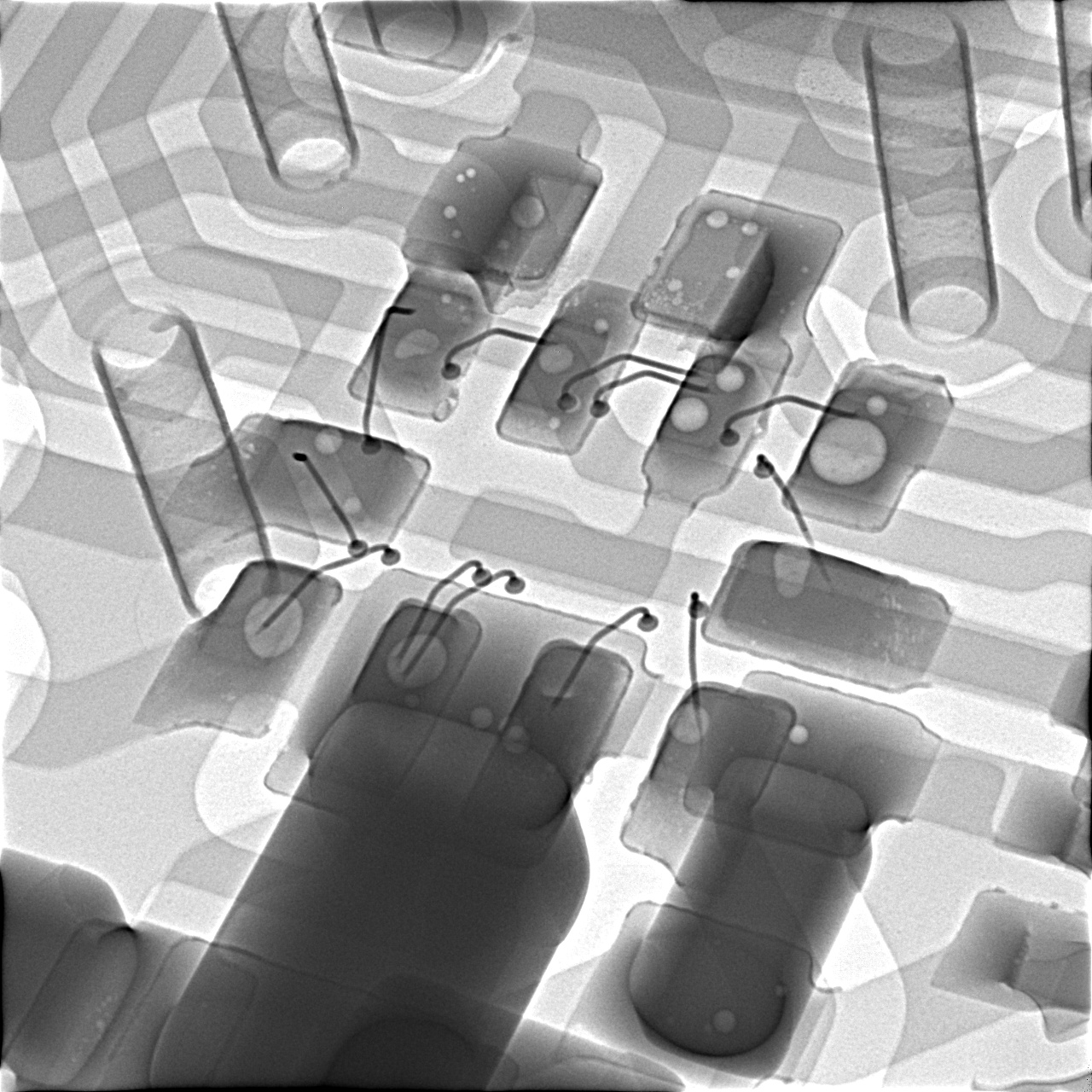
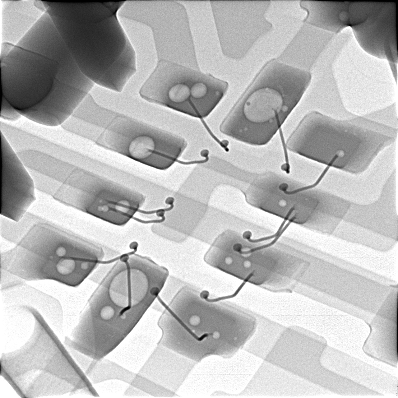
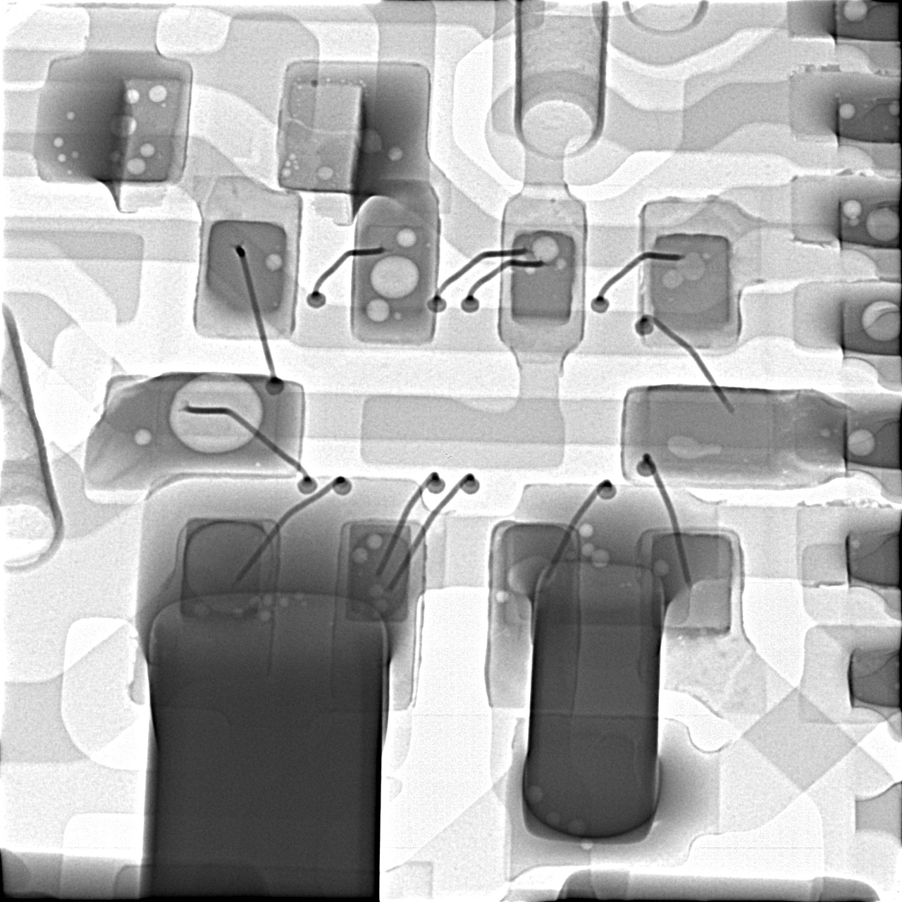
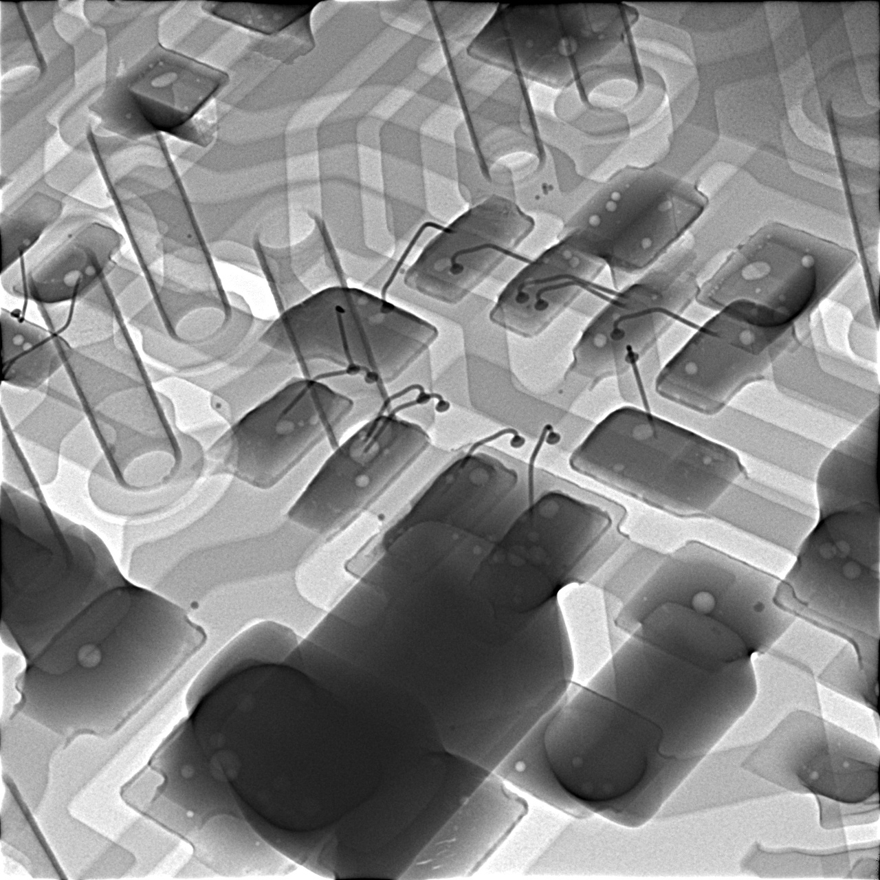
There is a component on each side of the card (one in TOP, the other in BOTTOM) and systematically the component on BOTTOM does not work after assembly in machine (the IC on the top side always work).
We replaced the components by hand, after which they work.

We are therefore thinking of a problem linked to the fact that the components on the BOTTOM side undergo twice the passage in the oven, unlike the components on the TOP side.
What do you think and do you have other possible explanations for our problem because in the current state of things we cannot start the production of our circuits?

Feel free to ask for additional informations if needed,

Thanks,
Cyril.

  • Cyril,


    You may want to try to adjust the amount of solder paste that you use for your second pass. Getting the right amount of solder paste is difficult for this device because of it's small size. Too much solder and the device can lift or tilt. Too little solder, and there may not be a reliable connection.

    Do you have any photos to look at for the failed boards? You might get a clearer picture of what's wrong after a good visual inspection.

    I have seen recommendations where smaller parts are placed on the first side of the reflow for two reasons. First, there may be deformations in the PCB after two reflows and second, smaller devices are less likely to fall off in the second reflow. However, I believe that the bottom side is your first reflow, and that's the side that's failed. If that's the case, you might want to do a visual inspection between reflows as well.


    Joseph Wu

  • Hi Joseph,

    The amount of solder paste is the same on the top side and on the bottom side. Should it be different because the bottom side undergo twice the reflow ?

    Here is two RX images that our manufacturer did.
    On the first one you can see the IC on the top side on the left and the IC on the bottom side on the right.
    The second image is another view of the IC on the bottom.


    Cyril.

  • Cyril,

    There appears to be some voiding in the solder underneath. You can see it in all of the pads to some degree. There could be problems with any part of the process, including the reflow, amount of flux or paste, and the temperature profile. A colleague pointed out the following application note:

    https://www.ti.com/lit/an/slua271b/slua271b.pdf

    It gives some guidance on the QFN package (as the package family for the ADS1118) and considerations for attachment in the manufacturing process. However, I'm not sure if we can provide much more guidance than the application note. 

    Joseph Wu

  • Joseph,

    Yes I saw the voids but the thing that bothers me is that voids are also present under functional ICs (on the top side) and that some non-functional ICs (on the bottom side) have fewer voids.

    Here is a RX image of a functional IC :


    And the following RX images are non-functional ICs :


    I designed my footprint according to the one given in the datasheet and my manufacturers have no clue of what's going on.
    So I guess that at that point I'll redesign my circuit either with the second IC also on the top side, either with another casing ... if it fits in the space that I'm allowed to use. I don't know just yet and I'll try to keep you informed.

    Cyril.

  • Cyril,


    I don't know the PCB manufacturing process very well, but it seems to me this is a manufacturing issue. Searching for the voids in the solder on the internet, I noticed these possible causes. I found these following comments here:


    https://www.7pcb.com/blog/how-to-prevent-solder-joint-voiding-cold-solder-defects.php

    • Too much flux is applied in the solder paste. The flux doesn’t have sufficient time to outgas before the solder has transitioned to a solid state.
    • The preheat temperature is too low so any solvent in the flux is difficult to vapour out completely.
    • The soak zone time is too short during the reflow process.
    • Lead-free solder typically has a 4% shirinkage in volume when it is cooled down to a solid state. It is possible to obtain voids when large pads are cooled down unevenly.
    • Paste oxidation occurs.

    If you have some sort of cold-solder joint in the process, the joint may look abnormally dull and you may lose connectivity. Here are some other causes:

    • The pre-heat time is too long and too high, preventing the flux from activating.
    • The solder paste has expired.
    • There is not enough heat absorbed by the solder.
    • The cooling speed is too slow

    Again, I don't have that much insight to the PCB process. At this point, I think you should ask the manufacturer about some of these possibilities. For the devices that aren't working on the bottom side, have you done a visual inspect other than the x-ray?

    Also, do you have any boards that pass with devices on the bottom? Is there a possibility of an error in the board?


    Joseph Wu

  • Joseph,

    We've visually inspected the boards before the X-Rays but did not notice anything wrong.

    We had 1 board out of 20 where the device on the bottom seem to pass.
    The first 10 boards were manufactured using vapor phase reflow, the next 10 using a "standard" reflow.

    I don't think there's a possibility of an error in the board as when we replaced by hand the devices on the first 10 boards, they then all passed.


    I will search for answers with my manufacturer and keep you updated.
    Thanks for your help.

    Cyril.

  • Hello,

    Just to give a few updates on the situation :

    I went back to my manufacturers and we tried a few things.
    We tried heating the ADS1118 again with hot air to melt the solder again but it didn't work.
    We tried this again but also adding solder but it didn't work either.

    We noticed that when we remove the ADS1118 the leads separate from the body of the component. So we're wondering if there is a problem with the alloys.
    I saw that the leads are NIPDAU. Our board finish is Ni-Au.
    My manufatcurer's expert on these questions is on holiday right now, he'll be back 24/08 so we wait for his view on the subject.

    Best regards,
    Cyril.

  • Cyril,

    I don't have any special details on rework of these devices. I do a lot of support for the ADC itself, but I'm not an expert in the manufacturing of boards and how to rework components on the board.

    I would wait for comments from your manufacturer's expert. In the mean time I'll see if I can find someone here that can comment on the packaging of this device and see if I can get recommendations.

    Joseph Wu