This thread has been locked.

If you have a related question, please click the "Ask a related question" button in the top right corner. The newly created question will be automatically linked to this question.

ADS131E04: Single ended input and input voltage range

Part Number: ADS131E04
Other Parts Discussed in Thread: ADS131M04

Hi,

I want to clarify some points regarding my input signal to ADS131E04.

ADS131E04 has a supply voltage of AVDD = 3.3 V and AVSS = 0 V. VREF is set to 2.4 V internal.
Assuming gain is set to 1, am I right that INxP is allowed to be in range from 0 to 2.4 V while INxN is fixed to 0 V? Or is the input range 0.8 V to 2.5 V? How does it look like for gain = 2? 0 V to 1.2 V or 1.3 V to 2 V?

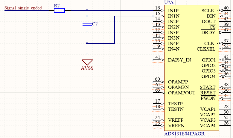
My "signal_single_ended" is conditioned to be in the range of 0 V to 2.4 V. Is it possible to convert the signal with a circuitry as simple as shown above? If not, how should I connect to my signal with the range 0 V to 2.4 V?
Is it possible to connect a single ended signal with the range of 0 V to 3.3 V directly and convert full scale?

Thanks very much.

Regards, Marko

  • Marco,


    If you have the gain set to 1, then the analog input range (where AINP and AINN can be) is AVSS+0.3V to AVDD-0.3V. However, the largest signal that you'd be able to measure is AINP-AINN = 2.4V. With AVDD=3.3V and AVSS=0V, you could measure 0.3V to 2.7V or you could measure 0.6V to 3.0V. The input is differential, so if AINN is higher than AINP then you would have a negative ADC reading.

    The range varies with gain because of the nature of the PGA. Normally, we describe this as the input common-mode range (see page 23 of the ADS131E04 datasheet). It describes the range with one equation as shown here:

    The reason the description is a bit complex is because there are a few things limiting the input range to make sure the PGA is operating correctly. The PGA basically looks like the front end of an INA and is shown in the datasheet as well:

    First the PGA has limits because of the opamps themselves. The output of the PGA won't go to within 0.3V of either rail (AVDD or AVSS). In gain of 1, the PGA can't buffer the input that close to either supply. When the gain is other than 1, the thing that limits the PGA is that the input and output common-mode signal must be the same. This is often something that seen in PGAs with high gain. When the output is large, the input must be much smaller. If the input common-mode voltage and output common-mode voltage are the same, and the output is large, then the input is limited to staying near the mid-supply point of the PGA. We don't have a diagram showing it for this datasheet, but I got this diagram from the ADS124S0x datasheet:

    It's similar in structure, but the PGA outputs go a little closer to the rails.

    For your application, you could use a different ADC that doesn't have this PGA limitation. The ADS131M04 is a similar device that amplifies the input, but doesn't have a traditional PGA for gain and doesn't have this limitation.

    Another option would be to use this device with a bipolar supply. This way, you could operate the device from +/-2.5V supplies. This way you could tie the negative input to ground and you'd be able to make measurements from there.

    The last option would be to build some circuitry that allows for the input to be translated to the right common-mode input level. If you used a fully differential amplifier, then you could set the input common-mode point to 2.5V and get a fully differential output signal.

    Joseph Wu

  • Hi Joseph,

    thank you, this helps a lot.

    When using the ADS131M04 my input range would be -1.2 V to +1.2 V with Gain = 1 and VREF = 1.2 V. Because my signal is between 0 V and 2.4 V I have to use a voltage divider and my conversion range will result in 0 V - 1.2V. A level shift to a higher common-mode input level is not possible (or not helpful) with ADS131M04 in my case. Am I right?

    Thank you.

    Best regards,
    Marko

  • Marko,


    The ADS131M04 doesn't have the same type of PGA as the ADS131E04. The ADS131M04 uses capacitive scaling to achieve the gain for the sampling. Because of this, it doesn't have the same common-mode input range limitations as the ADS131E04.

    For the ADS131M04, you could just use a voltage divider to divide the input to make the input to set the input as 0 to 1.2V. You would throw away half of the usable range (the negative inputs), but in practice, that may be easier to implement. This also reduces any problems of offset and drift that you might have from any level shifting circuitry.

    However, I'd note that the ADS131M04 has an input impedance of only 300kOhms. For your voltage divider, you'd need small resistors or the input impedance of the ADC loads the resistive divider (As an example, if you used two 10k resistors to divide the voltage, how much does 300k change the apparent 10k? It's about 3.2%).

    You won't have to worry about shifting the common-mode voltage of the input, but you might have to worry about the input impedance of the ADC.


    Joseph Wu

  • Joseph,

    thanks for showing these options and hints.