This thread has been locked.

If you have a related question, please click the "Ask a related question" button in the top right corner. The newly created question will be automatically linked to this question.

ADS131M08: Circuit design checked

Part Number: ADS131M08
Other Parts Discussed in Thread: REF3333, , ADS131E08, ADS1278, OPA350, REF5020, REF1930

Dear,

Can you checked and confirm schematic.

1) our every adc channel input is vary upto +/-2.8V sinwaveform.

2) We are applying external Vref +3.3V using REF3333 Ic.can we measure +/-2.8V sinwaveform. using this reference.

3) Do we required -3.3Volt to AGND for measuring  0 to -2.8V.

Sheet6, Analog Section-3.PDF

  • Rohit6230,


    At this point, the inputs are too large for the ADC to measure. First, here's a clip from the Recommended Operating Conditions from section 6.3 of the datasheet:

    First the absolute input range of the ADC only goes from AVDD to AGND-1.3V. The ADC will not operate with an input that goes to -2.8V. Again, the lowest it goes is -1.3V.

    Additionally, the voltage reference range is 1.1V to 1.3V (with a nominal voltage of 1.25V). Because of this, the 3.3V reference that you have selected is not in the operating range. I would note that if the reference is 1.25V, the input range will be only ±1.25V. Again, you won't be able to measure a ±2.8V input signal unless it is divided down, attenuated, and level shifted.

    I had some other comments about using 1uF decoupling capacitors for the supplies, a 220nF capacitor for the CAP pin, and using a common ground for AGND and DVDD (using a single plane for the ground). However, the input range for the ADC is the big issue that you have right now.


    Joseph Wu

  • Dear Joseph,

    That mean I can measure only upto +/- 1.25V if I will applied Vref 1.25V.

    As mention in Datasheet, ADC goes upto AVDD to AGND-1.3V, that mean if my AVDD is 3.3V, then can I measure sinewave on ADC input channel if this is in between 3V to -1.3V. also what should I keep my Vref pin condition in this case.

    Second condition can I measure 0-3 V at adc channel. if yes what should I keep my Vref pin condition in this case.

    Can you refer me TI 8 channel adc with simultaneous output who work on 0 to 3V.

  • Rohit6230,


    For the ADS131M08 the maximum reference input is 1.3V, so there's no way to measure a signal larger than ±1.3V, unless you were to use some sort of attenuation circuit at the input of the device.

    While the absolute input range of the ADS131M08 does include GND-1.3V to AVDD this means that either AINP or AINN can be at those voltages but the largest differential signal that you can measure is 1.3V. (Basically AINN=-1.3V and AINP=0V; or maybe AINP=3.3V and AINN=2.0V). The absolute input range is different than the full scale of the measurement.

    For the measurement you could set up a pseudo differential input, where you could use AINN=0V and then have AINP=±1.25V. Also you could use some AVDD midpoint so that AINN=1.65V and AINP varies from 0.4V to 2.90V (this way the input measures ±1.25V).

    However, if neither input setting works for you, I can think of only a couple other devices that have 8 channels and are simultaneously sampling, I would first look at the ADS131E08. This device's reference can extend all the way to AVDD. I would note that the absolute input voltage does not extend below AVSS (the presumed ground node). I'm not aware of many devices whose inputs extend below ground with a unipolar supply.

    The only other device that may work would be the ADS1278. This is a faster device, but it has a digital filter that imparts a significant measurement latency. I would note that this device requires a 5V supply.


    Joseph Wu

  • Dear Joseph,

    Thank you very much for response.

    I have update my design using ADS131E08. please check and confirm is that design is ok to read ADC input between 0 to 3V. with vref 3.3V

    Sheet2.PDF

  • Rohit6230,

    The ADS131E08 is a 64-pin TQFP device, while the ADS131M08 is a 32-pin TQFP device. Because of this the pins are mapped completely wrong. The two devices are not pin-to-pin compatible. First, I'd like you to correct your schematic to have the pins mapped correctly and I'll review the schematic afterwards.


    Joseph Wu

  • Rohit6230,


    One helpful source might be to pull up the ADS131E08EVM User's Guide and look at the schematic. It will show how much of the device is connected. 

    Also, you haven't mentioned what it is that you are measuring. It might help me later when I look at your schematic. Looking at what you have connected now, the AINN pins are connected to ground. I assume that your measurements will be single ended with AINP pins going from 0V to 3V?

    Joseph Wu

  • Dear Joseph,

    Thank you very much for update, Please find updated schematic pdf

    Please consider below points.

    1) our analog peak to peak signal is 3.0V max, normally we will measure signal from 0 to 3.0V directly through ADC and in that case we will keep open R11 resistor and short R15 with zero Ohm resistor. for this we will used extrenal Vref 3.3V.

    2)We are planning to used internal clock

    Please checked and confirm scematic.

    Sheet3-1.PDF

  • Rohit6230,


    I've looked through the schematic, and I have a few comments.

    First, look for C17 connected to VCAP1. This capacitance is recommended to be 22uF, and currently you have two 1uF capacitors in parallel. You want to increase that to the proper capacitance.

    It looks like your negative input is set up with a voltage divider. This is ok because the input impedance to the device is rather high, but you might want to use some precision resistors in case the exact voltage divider value is important or if the drift of this voltage matters.

    You'll want to make sure that the AGND and DGND are directly connected. In general, I think it's best to use a single continuous ground plane that AGND and DGND connect into. You can separate them, but we've found that it's easier use the single plane. If you're looking at the EVM as a guide, they do have separate grounds, but this is to accommodate the bipolar and unipolar supplies on the same board.

    Often, we use RC differential and common-mode filtering on the front end. For the differential filtering, we often use a bandwidth of 10x of the data rate. For the common-mode filtering, we'll use a bandwidth 10x-20x higher than the differential filtering.

    For the reference and supplies, I see that you've used some (presumably ferrite bead type) inductors. Generally, I wouldn't use inductors, because there will be digital currents, and these currents will have some periodic peak currents. This can cause the voltage to also periodically spike, when have this high L(di/dt). Generally for supplies, we only recommend the capacitors for supply bypassing. Unless the LDO and the reference datasheets recommend the inductors, I wouldn't use them there either.

    For the reference, I might consider using a lower noise reference if you need precision performance. The REF3333 has a higher noise than the REF50xx that was mentioned in the ADS131E08EVM User's Guide. Additionally, the User's Guide has a spot for an OPA350 as a reference buffer. The REF3333 has a typical noise of 92uVpp, which is rather high for a 24-bit ADC. This amount of noise is about the same as about 15uVrms of noise. If you had this amount of noise reflected into the input measurement, you'd probably be at about 17 bits of effective resolution just from the reference noise contribution.


    Joseph Wu

  • Dear Joseph,

    Please find changes in new schematic, we made one more change, our analog channel peak to peak input voltage between 0.2 to 2.8V. so we remove R11 and AGND R15. is it ok?

    Can we used internal clock using CLKSEL pin.Sheet3-3.PDF

  • Rohit,


    Earlier, I missed the input range specification for the ADS131E08 and your change of the AINN pins from the mid-supply point to ground just reminded me of that.

    First, the AINN input cannot be tied to ground. Ground is not in the input range of the ADC.
    This is because the PGA implementation is similar to that of an instrumentation amplifier and the input range and output range of the amplifier cannot be set that close to either supply. For this device, the closest the input can be is 0.3V above ground or 0.3V below AVDD.

    Also, the input range varies with the PGA gain. For the PGA, the input common-mode voltage is the same as the output common-mode voltage. As the PGA gain is applied, the input range will be smaller because the output range is limited by the output drive to the positive rail or ground.

    The common-mode input range is the following:

    However, I describe this in much greater detail in this post:

    https://e2e.ti.com/support/data-converters/f/73/t/925264

    For your setup, you could still use the voltage divider input to set the AINN input to mid supply. However, you would need to set the PGA gain to 1 and the input range would be set from AVSS+0.3V to AVDD-0.3V.

    If that doesn't work for you, I'll need to know more about your input and what you're measuring.


    Joseph Wu

  • Dear Joseph,

    Thank you very much for feedback, 

    if we used voltage divider input to set the AIxN input to mid supply. then do we need to apply -VSS( -3.3V ) supply  to our adc, because if INxP channel input is less than INxN input( voltage divider.) in that case my differential output is -ve voltage. and without -ve supply can adc measure that -ve voltage.


  • Rohit,


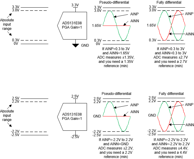
    I drew this set of input ranges for the ADS131E08. At the top is a unipolar supply running from 0V to 3.3V, at the bottom is a bipolar supply with ±2.5V.

    If you have inputs that go above and below ground, you'll need to use the bipolar supply (unless you're willing to put in sets of fully differential amplifiers or similar that can shift the input to the input range).

    So again, what exactly are you measuring? You haven't given me a description of the sensor being used.


    Joseph Wu

  • Dear Joseph,

    Thank you very much for explanation. I got your point.please find attachment of new design. We can used external reference or internal reference(Optional). with internal clock.

    Basically we are measuring output of thermopile sensor, Its sinusoidal output range between 0.4V to 2.8V with 1.65V mid point voltage.

    Sheet3-4.PDF


  • Rohit6230,

    I don't have to many comments for this schematic.

    First, the output capacitance of the REF5020 should be from 1uF to 50uF. However, you have about 70uF of bulk capacitance on the REF2.048V node. I would reduce the output capacitance to something lower, just to be sure.

    Another thing with the voltage divider from R11 and R15, you may want to use resistors with higher precision. I don't know if your divider needs to be exact, but you may want the precision to make sure that it doesn't drift around on you.

    One thing that might be helpful would be to get the ADS131E08EVM just to test your setup. The EVM GUI is a bit old and was developed in the Windows 7 era, but it should work on Windows 10 as well.


    Joseph Wu

  • Dear Joseph,

    thank you very much for your support,

    can we used REF1930 instead of voltage divider. It has 2 output so we can used 3V supply to our Analog section like opamp & sensors & 1.5Volt we can apply to -ve pin of each analog input channel.

  • Rohit,


    Using the REF1930 may be ok, but there are a few things that I wanted to point out.

    First with a 3V reference working as the new supply, you've just decreased the input range of the ADC. Originally the ADC supply was 3.3V, so the input voltage range was 0.3V to 3.0V (with a gain=1). Now, your range decreases to 0.3V to 2.7V. In the last post you mentioned that your input range was 0.4V to 2.8V with a 1.65V mid-point. This might make part of your signal range to large for the input of the ADC.

    Another problem might be the noise. The noise of this reference is 12ppm peak to peak. At 3V this would be 36uVpp and at 1.5V this would be 18Vpp. Depending on the OSR setting that you have, this might be a significant contributor to the noise (just compare this value to the noise you see in Table 1 of the datasheet).

    In general, I think using the reference in this way would be fine, but I would be concerned with the problems I mentioned above.

    Joseph Wu