This thread has been locked.

If you have a related question, please click the "Ask a related question" button in the top right corner. The newly created question will be automatically linked to this question.

ADC12DJ3200: signal looks AM

Part Number: ADC12DJ3200

I'm using Arria 10 example design provided by TI on customer board.
The example is has Signal Tap monitor JESD signals, in which rx_dataout
(240bit) from transport layer is also there.

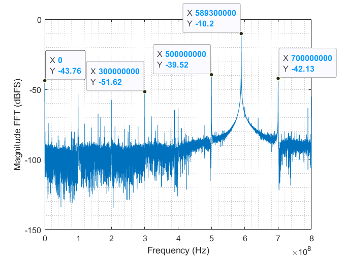
I have changed sample clock to 1.6GHz with SYSREF at 2.5MHz and the lane rate is 6.4Gbps.

I use Signal Tap to capture and monitor the data from ADC from rx_dataout by grouping it to ADC1 and ADC2 accordingly as JMODE2. Which is 120bit each.

Everything look good when using ramp (Reg205 = 0x4) and transport layer short test pattern (Reg205 = 0x5). Transport layer test pattern well aligned to rx_somfout on both ADC1 and ADC2.

Something interesting in normal mode, for example, ADC1 has signal input of 550MHz or 900MHz or 1270MHz or so,

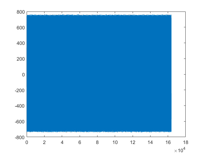
ADC1 data looks like AM (amplitude modulation signal but not constant sine wave from Signal Tap by setting the display to signed line. It's the same when plot the exported data in the time domain using MATLAB.

I need help about why is like this. Did I missing anything in configured ADC. Please note that the front end (ADC input) is the same as the EVM. Thank you.


  • Hi

    You will need unpack the lane data into samples according to table 23 in the datasheet.

    Regards,

    Neeraj

  • Yes, it's unpacked or interleaved according to table 22 (JMODE2, dual channel, 8 lanes).

    ADC2 has no signal and noise floor looks fine.  

  • This AM happens when input is 400MHz. It shows modulated with ~50MHz. 

    A couple of more questions:

    #1 about input coupling, it's DC-coupled as EVM does (0 ohm from Balun to the input pin).

    Should it be AC-coupled? 

    #2 the noise floor looks fine without signal in FFT. However it's not with signal, like "large skirt". 

    Again, have checked with transport layer test pattern and all samples are well aligned to SOMF.

    SOMF and SYSREF are locked to each other when set the SYSREF as the trigger in Signal Tap. (SYSREF is slower than SOMF). 

    Would this suggest the devclk, sysref and somf are fine? 

  • Any updates? Thanks.

  • Hi New2day,

    1. The AC signal you are sending to the ADC1 should be centered around 0 V( should have 0 v common mode).

    2. The FFT looks like a skirt because you are not using a coherent frequency for the input signal. Also your AC signal source and the clock source for the ADC should have a phase relationship between them( 10MHz locked with each other).

    Can you please send me the FFT of the signal you are seeing and time domain plots of the input of the ADC?

    Can you also let me know your Jmode, Dev clock frequency and K value you are using for ADC? Lastly please send me your register writes you are doing for the ADC. Also you can turn of the sysref to ADC and try to capture the data and see if you see any issues?

    Regards,

    Neeraj.

  • Hi Neeraj,

    1. the signal input to ADC1 is around 0V from signal generator. 

    2. please see attached FFT as example.

    3. is JMODE2, K = 4 at 1600MHz sampling clock (device clock). 

    4. ADC set-up.

    ADC12DJxx00
    0x0000 0xB0 // Do soft reset
    0x0200 0x00 // Clear JESD_EN (always before CAL_EN)
    0x0061 0x00 // Clear CAL_EN (always after JESD_EN)
    0x0201 0x02 // Set JMODE2
    0x0202 0x03 // Set KM1=3 so K=4
    //0x0204 0x01 // Use SYNCSE input, offset binary data, scrambler enabled
    0x0204 0x03 // Use SYNCSE input, 2's complement data, scrambler enabled
    0x0213 0x07 // Enable overrange, set overrange holdoff to max period 8*2^7 = 1024 samples
    0x0048 0x03 // Set serializer pre-emphasis to 3
    0x0061 0x01 // Set CAL_EN (always before JESD_EN)
    0x0200 0x01 // Set JESD_EN (always after CAL_EN)
    0x006C 0x00 // Set CAL_SOFT_TRIG low to reset calibration state machine
    0x006C 0x01 // Set CAL_SOFT_TRIG high to enable calibration

    Question:

    #1

    What did this mean "Also your AC signal source and the clock source for the ADC should have a phase relationship between them( 10MHz locked with each other)." 

    Did you mean that signal generator and the reference clock source should be locked to the 10MHz?

    #2

    did you mean turn off the periodical SYSREF to the ADC only? (not FPGA)

    Thank you.


  • Hi New2day,

    1. Your ADC clock signal and Input signal should be coherent with each and frequency locked with each other or you can use windowing and your spectrum will look as expected.

    2. From the figure of the FFT your capture looks fine. You don't have to turn off the periodic sysref to the ADC. BTW : the ADC will still capture without the sysref.

    Regards,

    Neeraj 

  • Hi Neeraj,

    1. what did "coherent with each and frequency locked" mean?

    Do we need to SYNC the signal generator with clock source (it's reference clock to the PLL)?

    2.Did you mean our FFT look normal?  

    There is a wide skit around the signal and spur level are very High. The noise floor does not look right neither - it's not acceptable to us.

    Was it not cause by periodical SYSREF? What could it be?

    Skirt normally mean there were missing samples.

    Thank you very much.

  • Hi new2day,

    1. Yes you will need to sync the signal generator with clock source and then choose a input frequency which is coherent.

    Can you send a time domain plot of the signal and also send the FFT of the signal without the analog signal applied to it. that will show me how the noise floor looks like.

    Regards,

    Neeraj

  • Hi Neeraj,

    1. about frequency coherent, could you give an example?

    - Our REF CLK to the PLL is 100MHz and sampling clock is 1.6GHz.

    - Out ADC input signal is 1.2GHz +/- 300MHz.

    2. In normal operation, the REF CLK in the system can be TXCO or a Synthesizer (its REF IN is 10MHz normally) but not signal generator.

    How would frequency coherent be accomplished between REF CLK and input signal?

    3. with frequency coherent, can the signal within 1.2GHz +/- 300MHz all be used (any frequency)?

    4. Please see attached time domain (ADC1) and noise floor on ADC2.

    Thank you.

  • Hi new2day.

    You don't have to use coherent frequency. I suggested that you use coherent frequency because you were seeing the skirt around your fundamental frequency as I mentioned before you are seeing the skirt because your input signal and clock signal or reference signal to PLL which generates the clock signal is not coherent. There are two way you can get rid of the skirt

    1. Use coherent frequency: again ref clock and Ain should be frequency lock with each other and you will need input a frequency which is bin centered which can be calculated based on following formula.

    Fs – the sampling frequency of the ADC.

    N – the number of points in the FFT. N must be a number that can be represented with a power of 2, such as 1,024, 2,048 or 4,096.

    Fin – the analog input frequency.

    RBW = Fs/N; bin number = Fin/RBW; Coherent Fin = round(bin number) X RBW.

    2.  Second method is use windowing: if you use windowing you don't need to enter coherent frequency. Your spectrum will look fine.

    Yes coherent frequency can be any frequency.

    The FFT looks good. If you are seeing higher than usual harmonics please make sure you are filtering the Analog input signal with a bandpass filter before passing it to ADC.  Calibrating the ADC might help with as well,

    Regards,

    Neeraj


  • Hi Neeraj,

    As you mentioned, we went through the MATLAB code again and found a error.

    The FFT plots look much better and no more wide skirt etc. There is Fs/8 spur at ~ - 53dBc ~-58dBc depending on the input signal level.   

    I think we need to tune some register settings.

    Any suggestions? Thank you.

    Regards,

  • Hi New2day,

    Did you calibrate the ADC after running it for several minutes? Please calibrate the ADC and let me know if you see better results? Also send me an FFT with the spur you are saying is higher than expected. 

    Regards,

    Neeraj

  • Hi Neeraj,

    I run the CAL every time changing the input signal.

    Did you suggest enabling background CAL?

    Please see attached plots. it's 156.25MHz spur at 1.25GHz sampling clock and become 200MHz at 1.6GHz, Fs/8.

    Thank you.

    Regards,

  • Hi Neeraj,

    Any updates? Thank you.

  • Hi new2day,

    I think the spurs are as expected and are within the datasheet number. I think the issue is your are taking the data as dBc and in datasheet the data is reported as dBFs. If you adjust for dBFs you will see the results as expected.

    Regards,

    Neeraj

  • Hi Neeraj,

    I ran a test with ADC IN signal generator 10MHz IN connected to REF CLK generator 10MHz OUT.

    There is Fs/8 spur at ~ 60dBFS (692.800 MHz (or delta freq: 200.000 MHz). ADC IN is 1107.2MHz with sampling clock at 1600MHz.

    JMODE2 is used in our case. See plot below.

    On page 16 of datasheet (JMODE3?), the SFDR is 69dBFS at Fin 997MHz and 66dBFS for Fin 2482, for example.

    Looks like we are 6dB away from the specification (above)?!

    1. what can we do to reach 66dBFS.

    2. do you have specification on JMODE2/0?

    Thank you.

    *********************************
    Analysis Results for: sn22984_sig1107m2_3dBm_VLP1350VLP1200_Fs1600_adc1adc2_Ref100m6dBm_Sync10m_ADC1.csv
    in directory: Z:\Modules\ANP\ANP500\Test\capture0916\sn22984\data\
    Analysis Results:
    Sampling Rate: 1600.000 MHz. FFT Points: 163750.
    Complex Flag: 0. 1 indicates Complex data. 0 is RealBin Resolution: 9770.992 Hz.
    Window used: HFT116D Flattop with the following Parameters:
    Window Gain: 1.221367e-05 ; Window Noise BW: 4.21864 bins.
    Input Signal Nyquist order: 2
    Script Run: ANP_500_data_analysis.
    Located in: D:\Design\matlab_scripts\ANP_500\ANP_500_data_analysis.m
    Script Version: 2.100000
    Script last Modified: 2020-09-16Script Run at: 2020-09-16  15:07:52
    *********************************
    DC Estimation. From Time Domain: -48.850 dBFS. From FFT: -48.688 dBFS
    Bin 1 w/o the real scale factor correction: -48.709 dBFS

    Signal Power -7.036 dBFS. Signal Freq (Nyq 1): 492.8000 MHz. Signal Freq (Act): 1107.2000 MHz
    Integrated Noise+Spur (NoiseBW corrected): -41.277 dBFS. Avg. Noise Floor: -84.157 dBFS

    *****  Detecting supplied frequencies and zeroing them before spur calculation ******
    Level must be 30.000 dB higher than -103.132 dBFS. That is higher than -73.132 dBFS

    Zeroed Out Known Freq: 800.000 MHz (Folded Nyq 1: 800.000 MHz). Level: -57.542 dBFS (or -50.506 dBc)
    **** End Detecting supplied frequencies and zeroing them before spur calculation ****

    *****  Detecting Harmonics and zeroing them before spur calculation ******
    Max Order: 20. Level must be 25.000 dB higher than -103.132 dBFS. That is higher than -78.132 dBFS

    Zeroed harmonic: 2. Freq: 2214.400 MHz (Folded Nyq 1: 614.400 MHz). Level: -74.157 dBFS (or -67.121 dBc)
    **** End Detecting Harmonics and zeroing them before spur calculation *****

    Spur1 Power -42.013 dBFS (or -34.977 dBc). Spur 1 Freq: 1.490 MHz (or delta freq: -491.310 MHz)
    Spur2 Power -57.844 dBFS (or -50.808 dBc). Spur 2 Freq: 0.892 MHz (or delta freq: -491.908 MHz)
    Spur3 Power -60.288 dBFS (or -53.252 dBc). Spur 3 Freq: 2.087 MHz (or delta freq: -490.713 MHz)
    Spur4 Power -60.514 dBFS (or -53.478 dBc). Spur 4 Freq: 692.800 MHz (or delta freq: 200.000 MHz)

    Average Noise Floor after signal & spur removal: -94.169 dBFS
    Integrated Noise after Signal & spur removal: -51.299 dBFS
    Remove all the excursions 10 dB above the Calculated Noise Floor.
    Recalculate Noise Floor.
    Integrated Noise Power (Noise BW Adjusted) after signal & spur & grass removal: -55.295 dBFS
    Average Noise Floor after signal & spur & grass removal: -98.139 dBFS
    *************************************


  • Hi Neeraj,

    #1

    Any updates? 

    #2

    Are the specifications on page 15, 16 of datasheet for JMODE3?

    Thank you.

  • Hi New2day,

    Fs/8 should be at 1200/8 = 150MHz. The SFDR you are seeing in the datasheet is a typical value so the value you are seeing is expected. Can you try backgound calibration and see if you see better results?

    The data on page 15 and 16 is for JMODE1.

    Regards,

    Neeraj

  • Hi Neeraj,

    Thank you for the patient. We are not satisfy the ~ 50dBc SDFR. 

    I have question about those CAL TRIM registers. 

    1. would it help by trimming the values of those registers, 0x07A to 0x095?

    2. was there any general rules for tuning those CAL TRIM registers? 

    3. what about offset filtering? 

    Thank you.

  • Hi New2day,

    Can you please remind me your max sampling frequency? 

    Regards,

    Neeraj

  • Our target sampling frequency will be 3.2GHz.

    However, the sampling clock used for the testing and the plots posted here (above) was at 1.6GHz.

    Like to know if there were general rules to play with those CAL TRIM registers (0x7A to 0x95).

    Also, the offset filtering, 0x97 and 0x98. Thank you.

  • Hi New2day,

    Can you try sampling at 3.2GHz instead and see if you see better performance?

    Regards,

    Neeraj

  • Hi Neeraj,

    I was planning doing so - test with 3.2GHz sampling clock still in JMODE2.

    In our real application or operation I'll need to use JMODE9 instead if increasing the sampling clock.

    I've changed the JESD settings to JMODE9 on both ADC and FPGA (Rx) according ADC datasheet and FPGA user guide.

    However, it didn't work.

    It seems there are some discrepancy about JESD204B parameters LMF etc. between ADC and FPGA so that mismatch happened.

    I like to check with you what should LMF be changed to from JMODE2 to JMODE9.

    Would it be exact the same as Table 18 in the datasheet or something else? Thank you.


  • Hi New2day,

    Yes you should use the exact same values for LMF as in Table 18. But please note some of the parameter( L and M are per link) So for JMODE9.

    L = 8, M= 2, F = 2, S = 4. Please make sure you are setting the proper K value for ADC and FPGA.

    Also note this is as decimation by 2 mode so your output datarate will be sampling frequency by 2.

    Regards,

    Neeraj

  • Hi Neeraj,

    In JMODE9, R=2.5, D=2, so for sampling clock at 3200MHz, the Lane Rate = (3200x2.5)/2 = 4000MHz. Right?

    Thank you.

  • Hi New2day,

    The Lane Rate = DEVICE CLOCK  x  R = 3200 x 2.5 = 8000Mbps.

    Regards,

    Neeraj 

  • Hi Neeraj,

    I thought you meant the lane rate needs to be divide by 2.

    My current JMODE9 FPGA project has L=8, M=2, F=2, S=4, K=31 with lane rate 3200x2.5=8000Mbps. FPGA clock = 200MHz (8000MHz/40).

    Thank you.

  • Hi,

    The lane rate should be 8000Mbps.

    Please note in the ADC when you set the K parameter it should be set to K - 1 on the ADC side. For example if you choose K = 31, the register 0x202 should be set to 30 or 0x1E.

    Regards,

    Neeraj