This thread has been locked.

If you have a related question, please click the "Ask a related question" button in the top right corner. The newly created question will be automatically linked to this question.

DAC80504: Problems interfacing with DAC80504

Part Number: DAC80504

Using and STM32 to control the DAC using SPI. I output does not change with messages, and reading DEVICE ID always gives corrupt data.

Procedure

  1. /CS
  2. Send GAIN configuration message (0x04,0x01,0x0F)
  3. CS
  4. /CS
  5. Send OUT0 DATA output request (0x08,0x0F,0xFF)
  6. CS

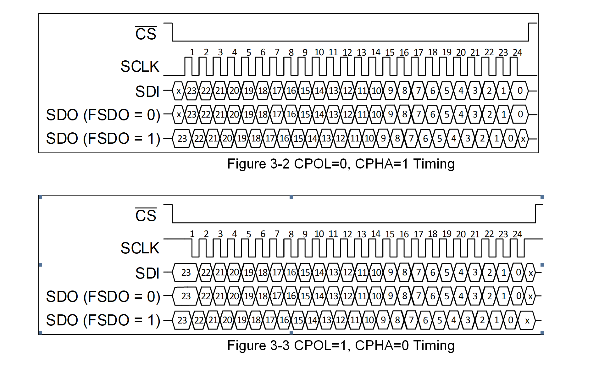
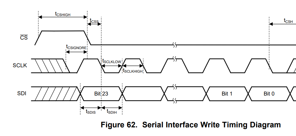
Writing is done to be sampled at CLK falling edge, as DIO spec says. 

Wiring


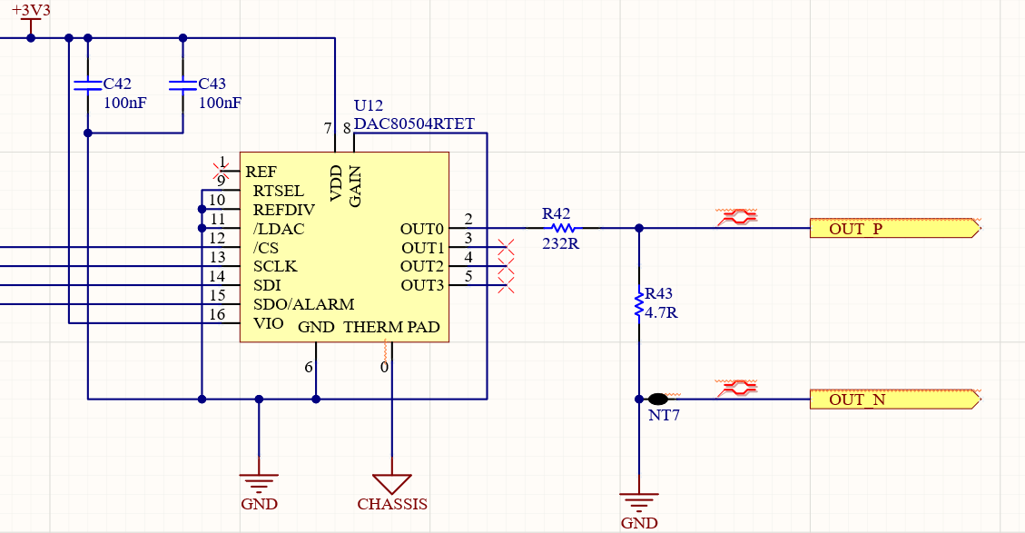
Signals coming into the device are confirmed to be properly routed.
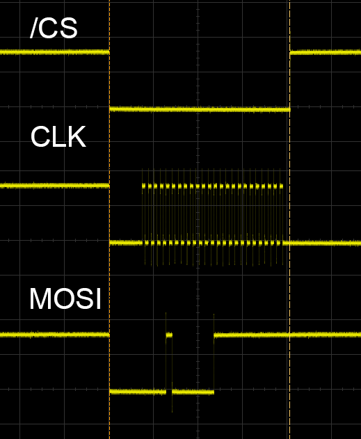
SPI Signals


overlay of /CS, CLK, and DATA. Data is sent MSB (bit 23 received first, and containing R/W message type)

Has anyone encountered an issue with this before, or am I missing something. Any help would be appreciated.

Thanks

UPDATE

I ran some trace tests and it looks like the first bit of the transmission is always ignored by the DAC. I capture the trace of the DAC SDO and the echo is always shifted one bit to the left, removing the 1st bit and moving everything else over. 

Changing my dataframe on the STM32 to fix this issue still eliminates the ability to read (first bit is never read by the DAC). 

  • Hi,

    Somehow the attached waveform pictures are missing from the post. Could you please reattach these pics?

    Also schematics of the DAC with STM32 controller will be helpful to look for any mistakes as well.

    Please share these details .

    Regards,

    AK

  • Hopefully the picture shows up now.

    Note my update which talks about receiving data from DAC SDO (echos of commands) always being shifted 1 bit left. I can read DAC SDO on the STM, and confirmed readings by taking traces so the STM32 is wired correctly.


  • Hi,

    whats the dev ID you are reading?

    Also are you able to get the device output as intended? or this is only while reading back the register ? Looking at your SPI frame, everything is fine to me.

    Data will be sampled on the falling edge as you mentioned. These devices supports SPI mode 1 and 2.

    Can you try some data output and let me know the results? Also please post the screenshot of the SDO , while reading the register.

    Regards,

    AK

  • Thanks for your help AK. Here is the latest trace with /CS, MOSI, and MISO. The CLK is green on each capture.

  • Hi,

    Looking at these scope shots, SDO is shifted by 1bit  looks like, am I correct? Whats the devID you are reading?

    As I see in your schematics, for reference min 150nF capacitor is required. Can you measure the voltage on Ref pin, it should be 2.5V.

    Also can you make the frame of SCLK in such a way that it starts at high and next fall edge is the MSB bit as per datasheet. In your scope shots, I can see SCLK is high and then brought to low , waiting for some time and taking to high.

    Basically what I am saying is /CS going to low to SCLK fall edge timing ( tss in datasheet), there is a min spec, in your case both are happening at the same time. Even if I take the first clock edge after this event, you will end up having only 23 clks and device will ignore the communication.

    Please see the below diagram for better understanding.

    Regards,

    AK


  • Looks like this was the problem; CLK must go low before /CS goes low (as shown in timing diagram from spec below. 

    Traces of updated /CS,CLK, and MOSI (MISO matches MOSI now):