This thread has been locked.

If you have a related question, please click the "Ask a related question" button in the top right corner. The newly created question will be automatically linked to this question.

DAC8551EVM: I can't get the Vout (Remains 0V)

Part Number: DAC8551EVM
Other Parts Discussed in Thread: DAC8551, DAC8550

I have DAC8551 Evaluation Module connected with TC-399 evaluation kit to drive analog voltage, I have connected DAC8551 Evaluation Module pins as following:
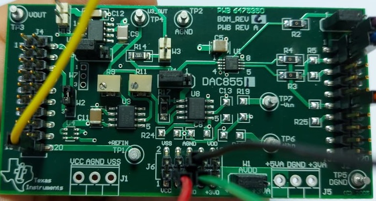
  1. Supply Voltage:
    1. J6-3: +5V (Vdd)
    2. J6-5: Gnd
    3. J6-6: Gnd
    4. J4-20: +5V (Vref)
  2. Jumper Setting Function Connections:
    1. W1: +5-V analog supply is selected for AVDD.
    2. W2: (1-2) Routes VOUTA to J4-2.
    3. W3: (Not connected) Disconnects VREFH to the inverting input of the output operational amplifier, U2
    4. W4: (3-2) Routes the user-supplied reference from U4 (if installed), TP1 or J4-20 to the VREFH input of the DAC8550/51/52.
    5. W5: (1-2) Negative supply rail of the output operational amplifier, U2, is powered by VSS for bipolar operation.
    6. W6: (1-2) CS signal from J2-1 is routed to drive the SYNC signal of the DAC8550/51/52.
    7. W7: (Not found) This is the default jumper position for DAC8550/51EVM when R1 is installed.
    8. W15: (Not connected) Disconnects the inverting input of the output operational amplifier, U2, from the gain resistor, R12.
  3. Serial Header Connections:
    1. J2-1: QSPI_CS of the MCU.
    2. J2-3: QSPI_SCLK of the MCU.
    3. J2-11: MTSR (SDI) of the MCU.

After done with this connections I run the software and transmit Din = 32768 to get Vout = +5V, but Vout still equal zero and I tried many values for Din and Vout still zero.

I expect output from J4-2 pin.

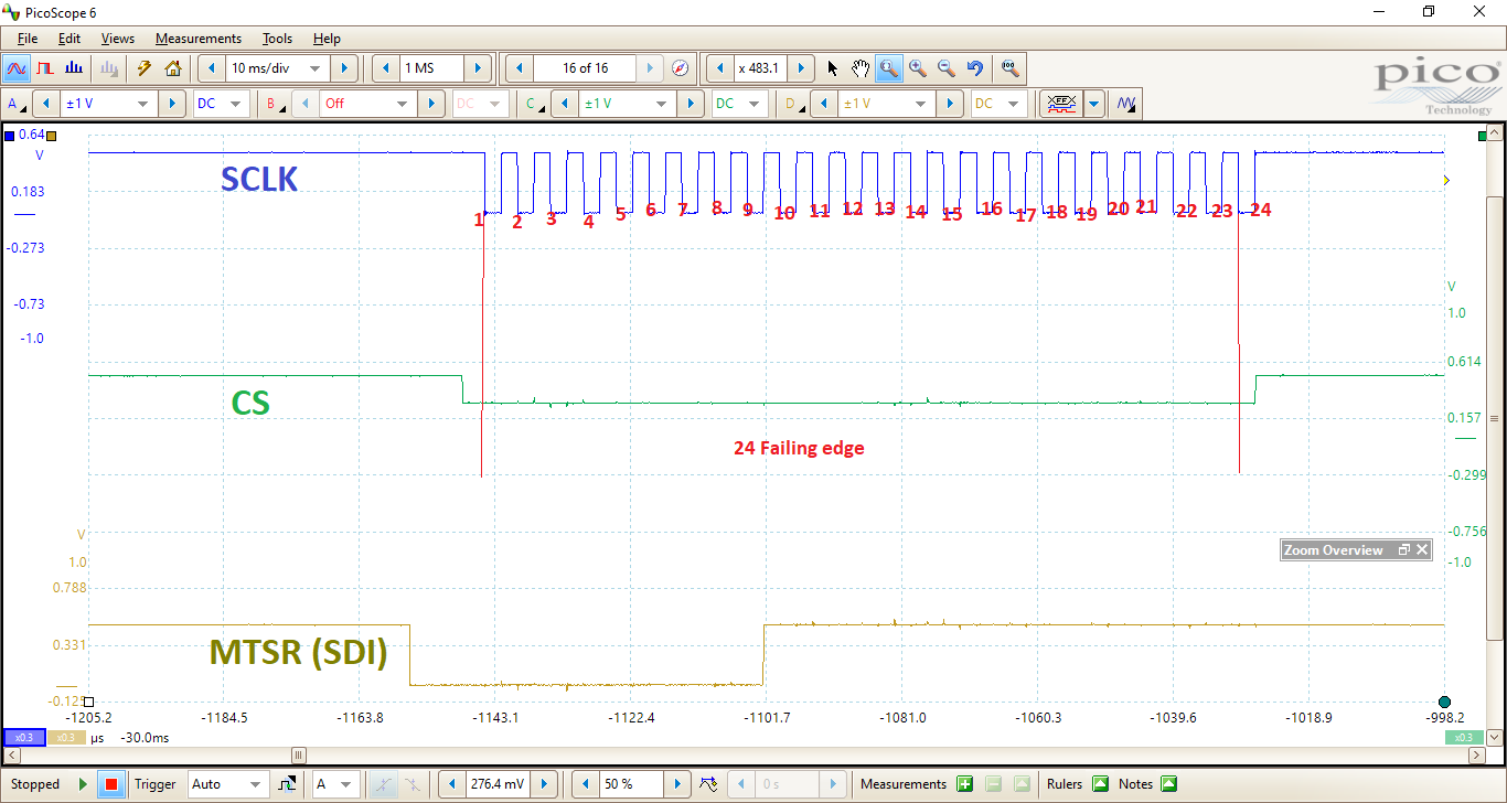
Note the QSPI output is tested and here is the output:
 

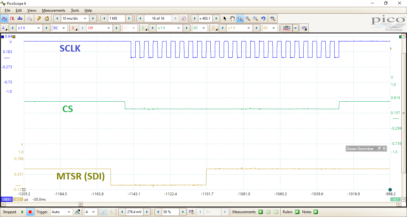
Could you please tell me if I have fault in connection or in using the evaluation module and help me to operate evaluation module to get the desired Vout.

Note: (I didn't use the operational amplifier so I expect Vout from J4-2 pin to get the DAC output before using the Op-amp also I didn't connect the VCC and VSS of Op-amp because I expect the output just after the DAC conversion)

  • Hi,

    Looking at the scope shots, I can see you have only 23 SCLK before your SYNC (CS) goes high ( Correct me if I am wrong here). In this case device ignores the communication.

    You need to keep the CS signal low for full 24 SCLK and we have timing requirements for last clock edge to CS going high.

    Please adjust the SPI frame accordingly and let me know the results after that. Have look at the datasheet snippet for better understanding.

    Regards,

    AK

  • The data sheet said "In a normal write sequence, the SYNC line is kept low for at least 24 falling edges of SCLK" and this is what happens in my oscilloscope snapshot.


  • Hi,

    Now its clear that You have 24 SCLk falling edges. I was not able to see the waveforms correctly. My Apologies.

    In your evm board, the onboard reference is assembled? If yes please remove the resistor R15. Other than this, I am not seeing any issues with your configuration.

    Can you please double check all the voltages are correct near to the DAC Pin, especially Vref? Also these waveforms are captured at the DAC side, right? ( Probe on those resistors labelled as R2, R3 , R4 )

    Regards,

    AK

  • R15 not found in the EVM, also all the voltages paths are tested to the pins of the DAC and test points found on the EVM.

  • Hi,

    I am assuming DAC is getting the Vref voltage as 5V. One quick thing to check out, whats the delay between 24th SCLK falling edge to SYNC rising edge,  Can you try giving some delay here? Say min 20ns?

    Regards,

    AK