This thread has been locked.

If you have a related question, please click the "Ask a related question" button in the top right corner. The newly created question will be automatically linked to this question.

ADC12DJ5200RF: Adc12dj5200RF multiple adc design

Part Number: ADC12DJ5200RF
Other Parts Discussed in Thread: LMK00304, LMX2594, LMK04828, LMK04832, DS90LV032A

Hi,

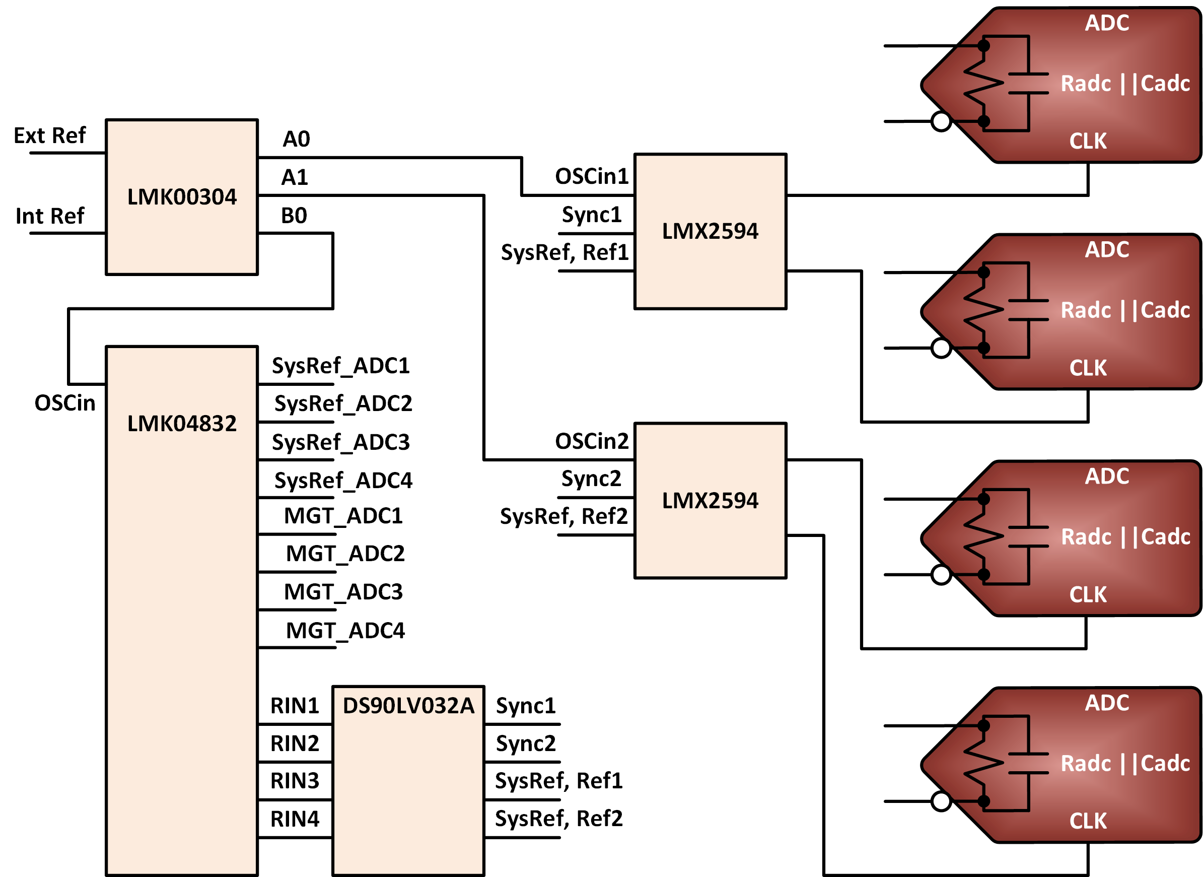
I am designing a multichannel receiver board with 4 nos of adc12dj5200RF. Kindly let me know if there is any reference design for the same.

Regards,

Pratiksha

  • Pratiksha:

     There is an EVM for the ADC12DJ5200RF, but there is not a reference design using four devices on one board.

    --RJH

  • Hi,

    Thanks for the quick reply.

    Kindly clarify the following queries.

    1. Is it mandatory to sync ADC regulators to an external clock (Referring to Page 11/13 of ADC12DJ5200EVM SCHEMATIC?)


    2. Kindly review the clock scheme attached herewith and let me know if any corrections are required. 

    Note: There is no provision for external RF clock. However, external RF reference will be available in the system. 

    Proposed clock scheme:

    1. LMK00304 receives an external clock reference and an on-board reference. Based on the select control, it selects either internal or external reference and generates two copies of the input signal.

       a. One copy is given to LMK00304, which generates two copies of the input signal. 

    i. The first output is given to one LMX2594, which outputs two RF clocks. These two RF clocks are given to first and second ADC as sampling clocks.

    ii. Similarly, the second output is given to second LMX2594 to generate two RF clocks. These RF clocks are given to third and fourth ADC as sampling clocks.

       b. The second copy is given to LMK04828. It generates the SYSREF signals for 4 ADCs, SYSREF for FPGA, MGT clocks for JESD data transmission and also generates SYNC and SYSREFREQ for LMX ICs.

    2. The SYNC signal generated by LMK04828 is buffered through LMK00304 to generate two copies of SYNC signal for the two LMX2594 ICs used for ADC sample clock generation.

    3. Similarly, the SYSREFREQ generated by LMK04828 is buffered through LMK00304 to generate two copies and given to the two LMX2594 ICs as SYSREFREQ input.

  • Hi Pratiksha,

    For question 1: Are you planning to put multiple switcher regulators on your power supply?

    For question 2: I will review your clock diagram and get back to you tomorrow.

    Regards,

    Rob

  • Hi,

    Yea.. Actually I am planning to go with the ADC12DJ5200EVM schematic for ADC power supply section. And also, planning to replicate the same power supply section schematic 4 times for the 4 ADCs.

    Regards,

    Pratiksha

  • Hi Pratiksha,

    That sounds fine for the power supply. Also, there is no need to synch these, you can expect the same performance regardless of sync.

    For the clock design, we believe there might be an easier way to implement this, I am putting a drawing together for you and will send it over later today.

    Thanks,

    Rob

  • Hi Pratiksha,

    See attached clock design.

    Regards,

    Rob

  • Hi,

    Regarding multichannel receiver module with 4Nos of ADC12DJ5200RF devices, I am planning to use 2 JESD lanes per adc. Hence, total 8 lanes will be required for 4 ADCs.

    The target FPGA has total 20 Transceiver Banks, with each bank having 4 Tx/Rx pairs.

    Kindly clarify the following queries.

    1. Kindly suggest the best way of connecting JESD lanes to the available Transceiver Banks.

    a. Making use of 2 Transceiver Banks(1st and 2nd ADC lanes to one transceiver bank & 3rd and 4th ADC lanes to second transceiver bank)

    b. Connecting each ADC JESD lanes to different Transceiver Banks.

  • Hi Pratiksha,

    Kindly let me know the FPGA chosen (and the lane rate). The simplest thing will be to use two Quads for the 8 total lanes. On the receiver side, you can use a single link with 8 lanes as the Rx IP. If the ADCs are synchronized using SYSREF, the Rx IP will compensate for the inter-lane skews and offer data of all the channels in an aligned manner, making down-stream signal processing easier.

    Regards,

    Ameet

  • Hi Ameet,

    The FPGA chosen is Kintex UltraScale KU040 FFVA1156. Date Rate will be 6.25Gbps/lane.(Considering Sampling Freq=5GSPS, Decimation Rate=32, No. of Lanes=2 with 64b/66b encoding)

    Regards,

    Pratiksha

  • Hi Pratiksha,

    At these lane rates, my previous recommendation should work. You can share one reference clock across the two Quads.

    Please note that if you generate the JESD Rx IP as multiple links, then it may not allow you to share lanes inside a Quad. That is often based on how the IP is architected, and each IP may reserve the Quad (and the associated QPLLs). At 6.25Gbps, I believe you may have the choice of either the QPLLs (shared for the 4 lanes) or the individual CPLL in each lane (channel).

    Regards,

    Ameet

  • Hi

    Thanks for the quick reply.

    Regarding the clock scheme suggested, Lmk04832 can support upto 7 SysRef outputs. But the scheme requires total 8 SysRef outputs. Kindly help.

    Regards,

    Pratiksha

  • Hi Pratiksha,

    I believe we provided a clocking scheme based on your requirements already.

    What has changed?

    Regards,

    Rob

  • Hi,

    There is no change in the clocking requirements. But, as per my understanding, RIN1, RIN2, RIN3, RIN4 should be connected to SYSREF outputs of LMK04832. LMK04832 supports maximum upto 7 SYSREF outputs, out of which 4 are used for ADCs SysRef generation  and 1 SysRef output is used for generating SysRef for FPGA. So, left with only 2 SYSREF outputs.

    Kindly help.

    Regards,

    Pratiksha

  • Hi Pratiksha,

    Thank you for the clarification.

    I will look into this and get back to you.

    Regards,

    Rob

  • Hi Pratiksha,

    Pratiksha Halijwale1 said:
    LMK04832 supports maximum upto 7 SYSREF outputs

    Unlike the LMK04828, every output on the LMK04832 can be routed as a SYSREF output, so actually the LMK04832 supports 14 differential SYSREF outputs.

    Moreover, the LMK04832 allows 3.3V LVCMOS format on odd-numbered outputs and CLKout8/10, and permits dual single-ended signals of the same polarity out of the CLKout/CLKout* pins (datasheet Table 25 for a complete description). Even more, the LMK04832 allows individual SYSREF outputs to be glitchlessly masked during operation, so that only certain outputs are active at a time (datasheet Table 22 for a complete description)

    By my count, you require 8 SYSREFs to the ADCs, 1 SYSREF to the FPGA, and 4 MGT_ADC clocks. This leaves one free LMK04832 output to handle the remaining SYNC/SYSREF_REQ operation to the two LMX2594. But you are not using the LMX2594 to generate SYSREF requests (diagram shows RFoutB going to an ADC), so actually you only need two LVCMOS SYNC signals. The remaining LMK04832 output can just be configured as two single-ended SYNC signals, and no DS90LV032A or any other buffer is required.

    Depending on which LMK04832 CLKout you use for the LMX SYNC signals, the other output in that pair may also activate and produce a SYSREF output. For example, if you placed your FPGA SYSREF on CLKout2 and your LMX SYNC signals on CLKout3, even if you masked the other SYSREF outputs, attempting to produce a SYNC signal from CLKout3 would also elicit a pulse from CLKout2. As long as your FPGA or ADC SYSREF input can be temporarily disabled or ignored while the LMX2594 SYNC is taking place, there should be no issues grouping them together. Afterward, you can set INPIN_IGNORE in the LMX2594 to ignore noise on the SYNC pin and power down the output format buffer for the SYNC signals, to avoid accidentally SYNCing the LMX2594 clocks while issuing SYSREF pulses.

    Regards,