This thread has been locked.

If you have a related question, please click the "Ask a related question" button in the top right corner. The newly created question will be automatically linked to this question.

ADS124S08: Measure the TUE using the ADS124S08 EVM

Part Number: ADS124S08

Hi,

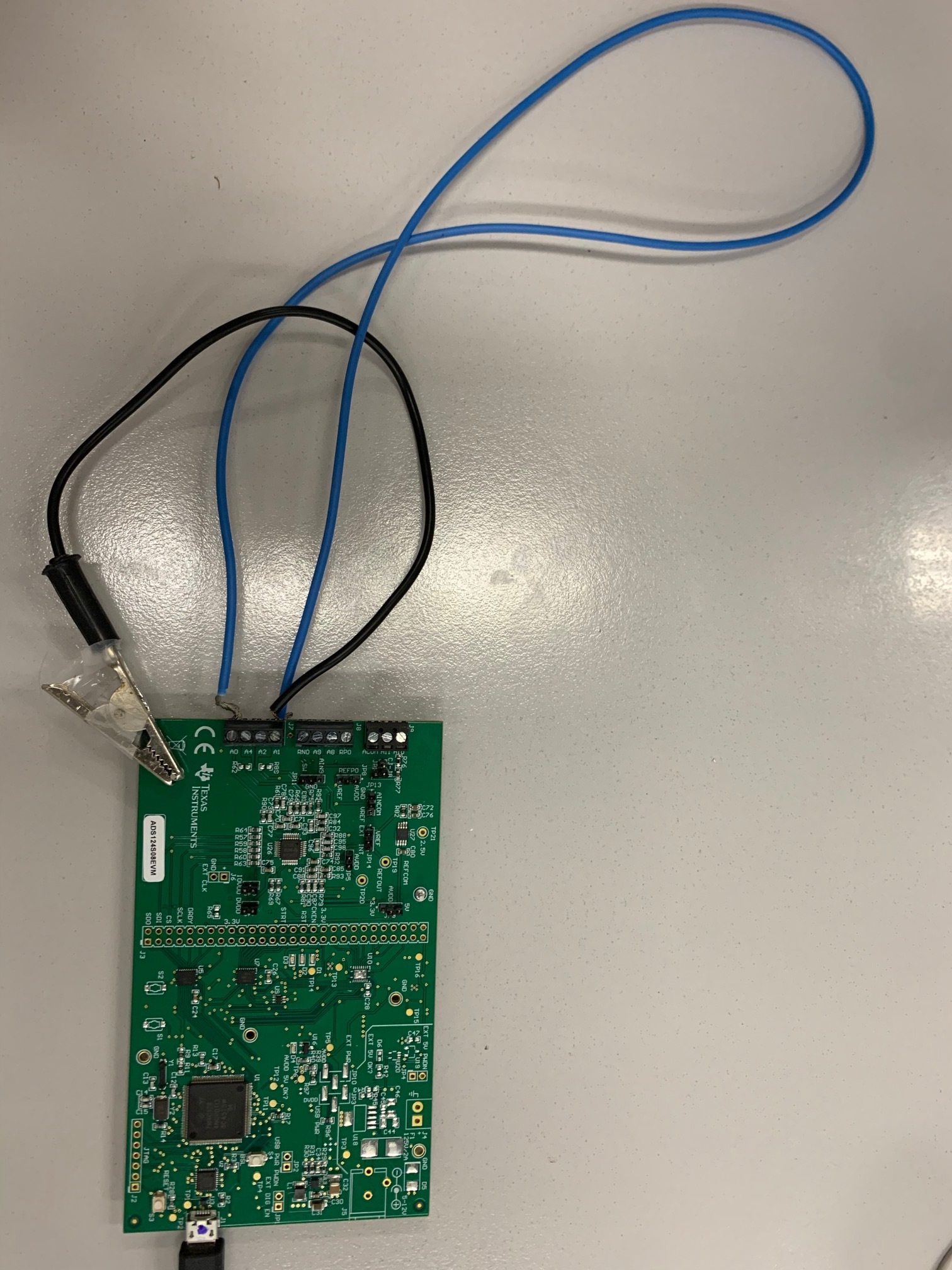
I am trying to measure the TUE of ADS124S08, and I got the TB-1 and TB-4 of J7 connected to the GND. And the result is shown as below. However, I got a few questions.

1.  I calculated the TUE using the max specs of ADS124S08(PGA gain is 1), as shown in the excel. And the result is 704 uV. But the test result shown above is 9 uV. I don't know why there is such a huge difference.ADS124S08 -.xlsx

2. The maximum data displayed as a decimal value in the 'Data Inspector' tab is 32. And I think it equals to code*Vref/PGA/(2^24-1)=32*2.5/1/(2^24-1)=4.8uV. But the maximum test result shown in the 'Time Domain' is 9uV. Is the difference because of the full scale range I used in my calculation? But the 'ADS1x4S08 Evaluation Module User's Guide' shows that 'The EVM is designed to be operated by using a unipolar supply. This means that AVSS is tied to analog ground and bipolar supply operation is unavailable on the EVM.' So I can't map 32 with 9uV and I got confused.

Thank you so much for your help and look forward to your reply.

Best regards,

Wendy

  • Hi Wendy,

    A couple of key points to remember is that when using the ADS124S08 device with a unipolar supply, the PGA must be disabled and bypassed when connecting the inputs to ground and the input range is still +/-Vref/(PGA Gain * (2^24 -1)) even for measuring single-ended inputs.

    Regarding question 1, when calculating the error you must make sure you are using the same units for each error source in the RSS analysis.  You show some as uV, some as ppm and some as a percent.  You may find the Analog Engineer's Calculator helpful for converting units.  Got to the Data Converters section and choose Conversions.  As far as worst case numbers, the TUE can always be worse than the actual measurement.

    Regarding question 2, as stated earlier the full-scale range is +/- Vref(PGA Gain * (2^24-1)).  When making single-ended measurements referenced to ground (AGND = AVSS = AINN) you essentially lose one bit of resolution as you can only measure up to the positive full-scale with AINP.  When using the 2.5V reference, the LSB value is 298nV (2*2.5/(1* (2^24-1))). 298nV *32 codes equals 9.5uV.

    According to the histogram data, there is 13 codes of peak-to-peak noise with a mean value of 23.6 codes.  So you would interpret this as an offset of 23.6 codes (7uV) with noise of 13 codes (3.9uV).  You can observe this in the time domain plot where the highest density lies around 7uV, and you can see that the noise ranges from not quite 9uV to slightly above 5uV.

    Best regards,

    Bob B

  • Hi Bob,

    Thank you so much for your help! I learned a lot from your reply.

    Besides, I want to make sure that is connecting the inputs to ground the appropriate method to test TUE?

    Also, I'm trying to design three-wire PT100 RTD measurement circuit with low-side reference and two IDAC current sources, using ADS124S08. And I learn it from the Analog Engineer’s Circuit Cookbook: Data Converters (Rev. A). But I got some questions and I want to learn from you.

    1. Determine values for the IDAC excitation currents and reference resistor

    In the circuit book, it directly choose the IDAC to be 1mA, and Rref to be 820ohm. And I don't know why. 

    2. Also in the circuit book, it says that the absolute input voltage must satisfy the following: 

    AVSS + 0.15V + [|VINMAX| • (Gain − 1) / 2] < VAIN1, VAIN2 < AVDD − 0.15V − [|VINMAX| (Gain − 1) / 2] 

    And I want to know how is the equation derived.

    3. Why the output voltage of the IDAC pin must be between AVSS and AVDD − 0.6V for an IDAC current of 1mA? I want to learn how is this relationship derived.

    Really appreciate your help!

    Best regards,

    Wendy


  • Hi Wendy,

    Here are some additional resources for you to review:

    Blog post on TUE

    TI Precision Labs

    A Basic Guide to RTD Measurements

    See my additional comments below.

    Best regards,

    Bob B

    Wenxiu Wang said:

    Hi Bob,

    Thank you so much for your help! I learned a lot from your reply.

    Besides, I want to make sure that is connecting the inputs to ground the appropriate method to test TUE? [Bob] The shorted input will only take into account offset error.  You will need see other associated error like gain error or any error related to the PGA.  So when testing, you may want to use something more practical as an input.  For simulating an RTD, you could use a fixed resistor value.

    Also, I'm trying to design three-wire PT100 RTD measurement circuit with low-side reference and two IDAC current sources, using ADS124S08. And I learn it from the Analog Engineer’s Circuit Cookbook: Data Converters (Rev. A). But I got some questions and I want to learn from you.

    1. Determine values for the IDAC excitation currents and reference resistor

    In the circuit book, it directly choose the IDAC to be 1mA, and Rref to be 820ohm. And I don't know why. [Bob] The IDAC current is arbitrarily chosen for a PT100 3-wire RTD.  The 3-wire RTD uses 2 IDAC sources to cancel the lead resistance from the measurement.  The total current is 2mA (1mA from each IDAC source).  The value of the reference resistor is chosen to center the input for the RTD at about mid-analog supply, which for this case uses 3.3V for the analog supply.  Setting the input at mid-analog supply allows for the best common-mode for the PGA at any gain.  Mid-supply for 3.3V is 1.65V and if we divide this voltage by 2mA we get 825 Ohm where a common value near this would be 820 Ohm.

    2. Also in the circuit book, it says that the absolute input voltage must satisfy the following: 

    AVSS + 0.15V + [|VINMAX| • (Gain − 1) / 2] < VAIN1, VAIN2 < AVDD − 0.15V − [|VINMAX| (Gain − 1) / 2] 

    And I want to know how is the equation derived. [Bob] This is the input range formula take from the ADS124S08 datasheet.

    3. Why the output voltage of the IDAC pin must be between AVSS and AVDD − 0.6V for an IDAC current of 1mA? I want to learn how is this relationship derived. [Bob] The 0.6V is voltage required to create a constant current source from the analog supply.  You can think of this as a control to adjust the current output and the control requires 0.6V to operate correctly.  If you attempt to have a constant current of 1mA through 5k Ohm with a 5V analog supply you will not see a 5V drop across the resistor, but instead something much less as the current source cannot drive all the way to the supply.  The larger the resistance the greater the error.  For example, 1mA and a 10k resistor would be 10V, but the analog supply is only 5V so this would not be at all possible.

    Really appreciate your help!

    Best regards,

    Wendy


  • Hi Bob,

    Really thank you for your help! It's really helpful for me.

    Today, I used the ADS124S08 EVM to test the RTD. And I got other questions that need your help.

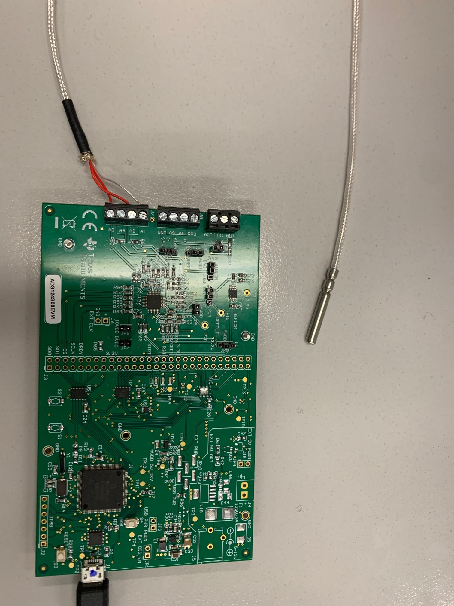
    1. I configured the EVM according to the picture below. And I got the result as attached and I changed the VRef to be 1mA*1kohm=1V. 

    According to the result, RRTD = (2 × R68 × ResultCODES / PGA ) / (2^24 – 1)=2*1kohm*3695881.5/4/(2^24-1)=110.14ohm. Are these analysis above correct?

    Besides, according to the test result, how can I calculate the TUE and noise? Since the result curve is appropriately straight down and I can't figure out where the highest density is.

    2. According to the EVM schematics, the EVM can only be used to test Three-Wire RTD Measurement, High-Side Reference. If I want to test 

    Three-wire PT100 RTD measurement circuit with low-side reference and two IDAC current sources, I need to draw another board like the picture below. Am I correct?

    Thank you so much for your help!

    Best regards,

    Wendy

  • Hi Wendy,

    You are correct in that the ADS124S08 is designed to make a high-side reference measurement for RTDs.  To maximize the various different sensor inputs, we used the high-side reference to demonstrate the use of this method.  If you want to make the measurement low-side you would have to create a new circuit path as you have mentioned in question 2.

    In response to question 1, yes your calculations are correct and for the time domain plot you would use the reference voltage at 1V.  However, for the RTD resistance calculation you would use codes regardless of the reference voltage as the measurement is ratiometric.  So in the time domain plot drop down option could could select codes.

    As to the variation you are seeing, you most likely are using the default of 20sps data output rate which takes approximately 102 seconds to complete.  So what you are actually measuring is the temperature drift of the RTD response.  So how would you determine the error of the conversion in this case?  You really cannot unless you stabilize the RTD temperature to a constant value such as in a temperature bath.  For now I would suggest limiting the number of samples to 128 and in this way it may be a little easier to detect the noise.

    So when you speak of TUE are you specifically concerned about the TUE of the ADC or of the system?  For determining the error we would normally use a precision resistor of fixed value as the sensor to be excited.  The resistor is a high quality resistor such as a Vishay Y6071100R000T9L.  This removes any error of the RTD and limits the temperature effects to that of the limits of the precision of the resistor.  Customers sometimes use an RTD calibrator which will introduce some error but the output will be stable as compared to an an actual RTD.

    When determining the total error, the reference precision and stability directly affect the ADC result as well.  The resistor used on the EVM is not highly precise (1k +/- 0.1% with 25ppm per deg C temperature coefficient).  The reference resistor will add some error relative to potential gain error.  Replacing the resistor with a higher precision will improve the TUE.  Also, by using a second fixed resistor of a different value for the RTD input will help to determine the offset/gain error of the system.

    Best regards,

    Bob B

  • Hi Bob,

    Thank you so much for your help. I have learned a lot from your comments!

    Best regards,

    Wendy

  • Hi Bob,

    Also in the Analog Engineer’s Circuit Cookbook: Data Converters (Rev. A). https://www.ti.com/seclit/wp/slyy138a/slyy138a.pdf?ts=1602250704946, the Three-wire PT100 RTD measurement circuit with high-side reference and two IDAC current sources, it says 'RBIAS is selected to set the input to the mid-supply voltage. ' However, the RBIAS is set to be 1.1kohm, and the VAIN2 and the VAIN3 are 1.3V and 1.1V, respectively. While the supply voltage is 5V, VAIN3=1.1V is far from the mid-supply voltage. Could you please help me with the question?

    Best regards,

    Wendy

  • Hi Wendy,

    If you re-read the entire section you will see the reasoning behind the value chosen.  The explanation is as follows:

    4. Set RBIAS and verify that the design is within the range of operation of the ADC. Once the reference resistance, IDAC current magnitudes, and ADC gain are set, select the RBIAS resistance to set the bias voltage of the input measurement. Normally, RBIAS is selected to set the input to the mid-supply voltage. However, there is a large total sum of the voltage drop across the reference resistor, the RTD resistance, the bias resistor, and any optional input protection used in the circuit. It is important that the RBIAS input offset is high enough to keep the RTD measurement voltage in the PGA input range, but not too high so that the excitation current output pin is within the compliance voltage of the IDAC. Setting RBIAS of 1.1kΩ meets this requirement.

    The remaining section discusses how the value was derived.

    Best regards,

    Bob B

  • Dear Bob,

    Thank you so much for your kind help!

    Best regards,

    Wendy