This thread has been locked.

If you have a related question, please click the "Ask a related question" button in the top right corner. The newly created question will be automatically linked to this question.

ADC12DJ5200RF: issues

Part Number: ADC12DJ5200RF
Other Parts Discussed in Thread: ADC12DJ3200

Hi team,

Another customer asked about ADC12DJ5200RF, sorry to disturb you again.

The customer problem is described as follows:

1. ADC is ADC12DJ5200RF and configured as JMOD1. The code of Transport Layer is written with reference to the example project of ADC12DJ3200. After careful check, no problem is found.

2. When JTEST=Ramp test mode, the data read out is correct, indicating that the link is correct.

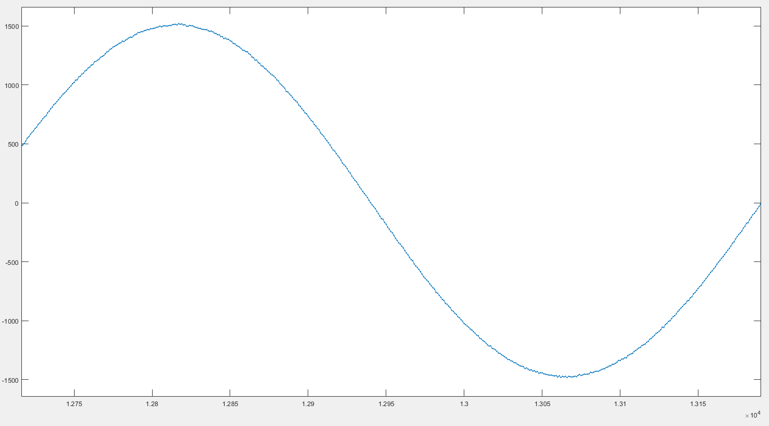
3. After changing to JTEST=nomal mode, it is found that only part of the output waveform of the Transport Layer is correct sine wave (the output is 240bit, divided into 20 channels * 12bit), and the rest are wrong. Some waveforms are as follows

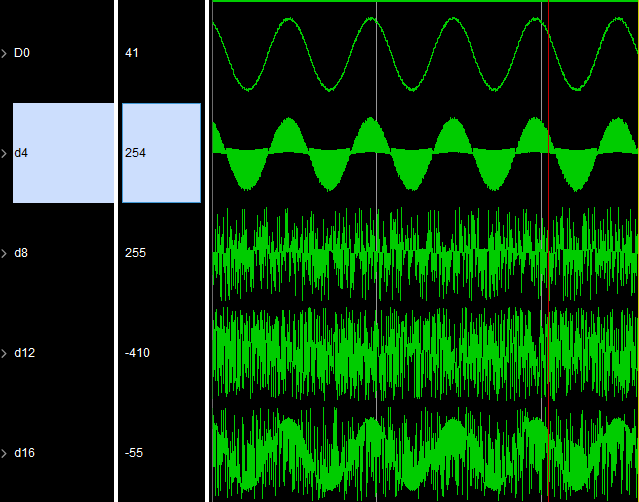
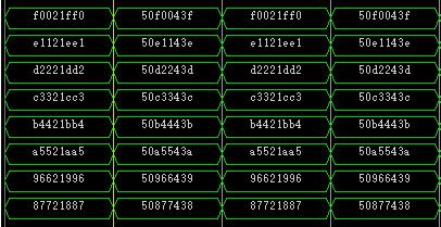
4. In order to locate the problem, I configure JTEST=Transport Layer test mode, observe the data received by lane0 ~ lane7, and see that the test data is wrong. It is different from the description in table 61. Short transport test pattern for n '= 12, f = 8 modes (length = 1 frame) in the datasheet. It seems that the data is just misplaced

As shown in the figure: (From top to bottom, it corresponds to DA0 ~ DA7 of table 61)

The difference between Transport Layer test mode and Ramp test mode is whether the Transport Layer is included. Does this mean that there is something wrong with the Transport Layer? What are the possible causes?

  • Hi Amy,

    No problem, I will have to look into though for you.

    I will get you an answer tomorrow.

    Regards,

    Rob

  • Hi Rob,

    I'm the customer Amy was talking about. Thank you for your reply.

    I have solved the problem now. Just reverse the order of every octets to get the correct test data, and now I see the correct sine wave on the screen.

    But a new problem is beginning to bother me and I would be very grateful if you could give me some advice.

    Here are some descriptions of the problem:

    1. JMOD=1, and  two RX cores were used to accept data from 16 lanes in FPGA. I sort all the data according to the format in Table 28 and draw the waveform:

     It appears that the time interval of TI ADC is wrong.

    2. I have confirmed the order of the data by check the Test data of the Short Transport Test Pattern.

    3. If data from only one RX core is used to plot, its waveform is fine, as shown below:

    I hope you can give me some Suggestions. Looking forward to your reply. Thank you again!

    Regards,

    我好菜啊

  • Hi 我好菜啊,

    Are you using two links or one?

    If two, then what might be happening is there one link is off by a sample or two.

    You can try collecting both links in the data capture and moving one or the other to see if that lines things up.

    Keep me posted and let me know if that works.

    Regards,

    Rob

  • Hi Rob

    Thank you for reply.

    Yes, we using two links and each link is connected to one RX core.

    We try to move  link B one frame(40 sample), and the waveform is correct (using yesterday's data).

    But this is not always the case. Sometimes the data is correct, two links don't have a misalignment of  frames.

    Here's another clue that might have something to do with this problem: We don't send sysref to the ADC, because something wrong with it. The link can up without sysref so we didn't handle it.

    Can LMFC without synchronization cause this phenomenon?

    Regards,

    我好菜啊

  • Hi 我好菜啊,

    The problem now is the FPGA ref clock, is not being distributed internally in the FPGA to each of the quads.

    For example, if the ref clock comes into qual0, then gets pushed to qual1, and then to quad2 and so on, there is too much delay.

    It would be better for the ref clock to enter the FPGA, then be split into four replica outputs/fanout buffer, then each output routed to each quad used.

    Regards,

    Rob