This thread has been locked.

If you have a related question, please click the "Ask a related question" button in the top right corner. The newly created question will be automatically linked to this question.

ADS1262: Schematic validation needed

Part Number: ADS1262

Hi All,

This is the first time we use the ADS1262.

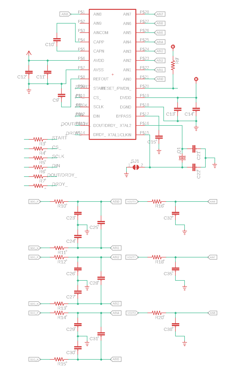
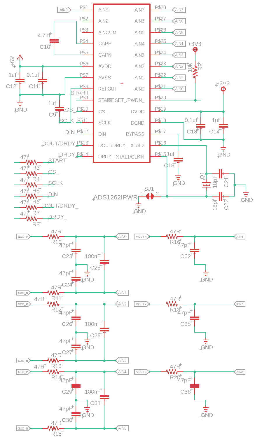
Our requirement is to use 3 differential ADC channels and 3-single end ADC channels.

So, we have configured pins A0 to A5 for differential channels and A6,A7,A8 for single-ended input ADC's as shown below.
We have designed for single mode supply (no -ve voltage) only +5V for ADC  reference and 3.3V for Digital.

Can any of you please confirm is our schematic design fine to meet our requirement?

  • Hi Srinivasarao,

    Your schematic looks correct in its implementation. Without knowing the passive values it will be hard to comment further, but as long as you followed the datasheet recommendations you should be okay.

    -Bryan

  • Hi Bryan,

    Thanks for the reply. Please find the updated schematic below with values.

    Our project requirement demands 3-differentials and 3 single-ended channel ADCs. So, we are comfortable in designing the differential as we use both channels(AINN,AINP). But to achieve the other 3 single-ended channel ADCs, we are not sure how to go about it.

    Once consume 6 ADC channels for 3 differential-end ADCs, we are left 4 ADC channels to meet 3 single-ended ADC channels requirement.

    As per the datasheet to use single-ended channel ADC the other unused input channel should be tied to 2.5v reference output voltage incase operating with single 5V supply. If I follow this I will achieve only 1-single-ended channel ADC and left one channel idle. 

    We would like to use PGA for single-ended channel configuration.

    In Our design for single-ended channels we are left AIN6,AIN7,AIN8,AIN9. So, can we connect AIN9 to 2.5v and use AIN6,AIN7,AIN8 as single-ended input channels and use multiplexing to configure AIN6,AIN9 and AIN7,AIN9 and AIN8,AIN9 as sets to achieve single-ended channel configuration?


  • Hi Srinivasarao,

    Your schematic still looks good, all of the values around the ADC look like you followed the datasheet recommendations very closely - thanks!

    The input filter resistors look like they might be a bit small (e.g. R14 and R15, R20, etc.) We usually see larger resistances (1k to 4k) in the input path as this helps limit the current into the ADC in the case of an overvoltage event. The ADC absolute maximum pin current is 10 mA, so you want to make sure that is never exceeded. However, if you are certain that your system will not see such potential errors, then these resistors could be acceptable.

    For the filter cutoff frequency, the differential filter (e.g. R14 + R15 & C31) is giving you a cutoff frequency of approximately 16 kHz, which is okay. But the common-mode / single-ended filter (R13 & C29 or R20 & C38) cutoff is 72 MHz, which is not providing any anti-aliasing. I would suggest reducing the cutoff frequency of this filter by increasing the cap size to at least 10 nF (it is usually 10x smaller compared to the differential filter cap). You could also reduce the differential filter cutoff accordingly, depending on how fast you want to sample.

    You are correct in that you can use AIN6, AIN7 and AIN8 as the single-ended inputs in your system, and measure them against AIN9 (in reality, every measurement made by the ADC is between AINP and AINN, so they are all differential measurements as far as the ADC is concerned). AIN9 can be connected to ground (single-ended) or some voltage (pseudo differential). Just make sure to keep within the ADS1262 PGA's common mode range, per equations 12 and 13 in the datasheet.

    -Bryan

  • Hi Bryan,

    Thank you for the response. 

    Can you please let us know if we can leave the AINCOM pin float or do we need to connect it to any supply to meet our design requirement?

    Please suggest.

  • Hi Srinivasarao,

    The AINCOM pin is just like any other analog input, so you can follow the recommendations outlined in section 10.1.7 in the ADS1262 datasheet. This suggests to tie unused analog inputs to mid-supply.

    -Bryan