This thread has been locked.

If you have a related question, please click the "Ask a related question" button in the top right corner. The newly created question will be automatically linked to this question.

ADC34J45EVM: JESD204B interface with ADC34J45EVM and ZCU106

Part Number: ADC34J45EVM
Other Parts Discussed in Thread: ADC12DJ3200, ADC12DJ3200EVM, ADC34J45

Hello,

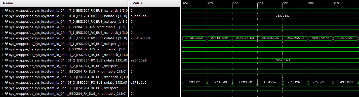
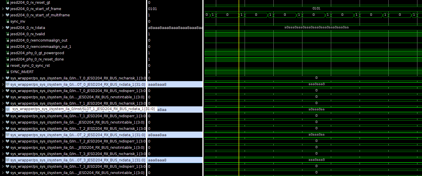
I previously posted a question about SPI configuration for the ADC34J45EVM, and now I'm having some problems trying to implement the JESD204B interface itself. I'm using the Xilinx JESD204 IP cores, and tried interfacing to the EVM in Subclass 0, 20x mode (LMFS= 4421), 3.2 Gbps, at 160 MSPS. The FPGA RX is configured as:

  • L=4,F=2,K=8
  • The core clock (x40) is at 80MHz, and is derived from the 320MHz clock the LMK generates for the transceivers.
  • SYSREF is sampled at the positive edge
  • Core re-aligns LMFC counter on all SYSREF events
  • SYSREF is not required after re-SYNC (RX core deasserts SYNC on the next LMFC)

I think configured the Xilinx IP cores correctly (I have made a similar post on the Xilinx forum, so I think I'll get confirmation/corrections soon), but I cannot get the link to work properly (it sometimes achieves SYNC briefly, but keeps losing). The basic steps my system goes through are:

  • Configure the EVM through SPI, following one of the config files provided by TI (ADC3xJxx_160MSPS_Operation_LMK_Setting.cfg)
  • Reset JESD IP cores
  • Write write AXI config to IP cores
  • Soft reset the IP

I'm quite new to JESD204B, so I'm not sure if I made any obvious mistake. Also, I'm not very familiar with the LMK chips. With that in mind, questions are:

  1. Am I correct in assuming I can simply follow the .cfg when programming the LMK? In the SPI configuration step, I simply configure the registers as described by the file, in the same order. Looking at the datasheet, it seemed very complex (and my chronogram is tight), so I'm trying this simplistic approach to at least get the link working before delving into the LMK details. I'm aware that simply blindingly following some file is... unusual, so I'm expecting there might be something more
  2. Is this configuration achievable? The Xilinx IP work in x40 rate exclusively. I'm new to JESD204, so I'm not sure if this is compatible with the x20 mode in the ADC. Although from what I understand there seems to be nothing prohibiting this, I'm not confident enough in this.

  • Hi Laez,

    If you are using the configuration file "ADC3xJxx_160MSPS_Operation_LMK_Setting.cfg", then the ADC is configured in 20x mode for JESD.

    To configure the ADC for 40x mode, please write to the ADC:

    (register data)

    0x2B 0x01

    0x30 0x03

    However, if you look at page 53 of the datasheet, 40x mode can only sample up to 80 MSPS, so you will need to use 20x mode for sampling at 160 MSPS.

    Best,

    Dan

  • Laez,

    See if the attached document helps. This may help with setting up the LMK for a 160Mhz sample rate for the ADC. 

    Regards,

    Jim

    ZC706 ADC34J25 160 4421 Setup.pptx

  • Hi Dan,

    Thank you for the fast response.
    I'm aware that this file configures the ADC for x20 mode, and also that x40 mode only goes up to 80MSPS. Perhaps I didn't express myself correctly, but with question 2 in the post I was asking if the configuration of an x40 RX on the FPGA and an x20 ADC TX was achieavable. Is such a thing possible?

    Regards,
    Laez

  • Hi Jim,

    Thank you for the document, it does clarify some things with respect to LMK configuration. I guess that it also hints that the response to my question 2 is that yes, the configuration is possible. However, I'm not currently using the interposer or the HSDC pro GUI, instead I'm trying to develop a custom FPGA solution. Do you have any Ultrascale-based reference designs?

    Thank you,
    Laez

  • Laez,

    We only have example KCU105 firmware code for the ADC12DJ3200. You can find this under the ADC12DJ3200EVM product folder on the TI website.

    Firmware that was used with the interposer card be found under the TSW14J10EVM product folder.

    Regards,

    Jim

  • Jim,

    I've looked at the firmware example, and also at the HSDC pro files. Notably, I found some configuration files for the ADC34j45EVM in the HSDC pro software, and also a post in the forums (e2e.ti.com/.../605740), which details some suggested working configurations for this board (which, according to the TI employee, correspond to the 'all zeros' ADC configuration state that the .cfg I mentioned earlier):

    JESD IP Core_CS=2
    JESD IP Core_F=2
    JESD IP Core_HD=0
    JESD IP Core_K=10
    JESD IP Core_L=4
    JESD IP Core_M=4
    JESD IP Core_N=14
    JESD IP Core_NTotal=16
    JESD IP Core_S=1
    JESD IP Core_SCR=0
    JESD IP Core_Tailbits=0
    JESD IP Core_LaneSync=1
    JESD IP Core_Subclass=1

    However, following this still does not seem to work. Looking at the data sheet for the converter, some questions arise.

    • What is the K value? In the ADC34j45 datasheet, there seem to be two conflicting descriptions of the default value in the "all zeros" sate: in the description of register 0x2B it seems to state that K=9, but on the description of register 0x31 K=8 is implied. To make matters worse, the forum post suggests K=10 (this matches the LMK SYSREF period when using the .cfg above). Which one is correct?
    • In the datasheet, register 0x34 of the ADC34j45 (which sets the subclass), seems to specify Subclass 0 when written 0. This goes against the post and the HSDC pro example, which suggest Subclass 1. Which is correct?
    • In the mentioned forum post, it's stated that SYNC polarity is inverted in the EVM. Looking at the board schematics, the traces SYNCP and SYNCM do seem to be switched. However, just to be certain, I want to make sure if I'm not "double correcting" for this issue: the Xilinx JESD204 IP uses a SYNC signal that goes low when requesting for CGS, do I need to invert it in order to compensate the inverted traces on the EVM, or is the EVM inverted already to compensate for an inverted behaviour between the JESD IP and the ADC?
    • What does LaneSync=1 imply? I didn't find any related setting in the JESD IP core.

  • Laez,

    I agree the data sheet has a few issues. Please set all ADC registers to 0x00. Use a K value of 10 for the FPGA. Set the FPGA to use subclass 1. By default, even with the ADC subclass set to 0, register 0x3b will be set to reset all clock dividers on every sysref pulse.

    The SYNC is inverted on the board so you must have your firmware take care of this inversion. That is what the HSDC Pro software/firmware does with our setup.

    Ignore Lanesync. This is a feature used by HSDC Pro only. 

    Regards,

    Jim

  • Hi Jim,

    I've done what you recommended and now I'm able to get through ILAS, and receiving data. I did have some problems with K: at first, when I set the FPGA to use K=10 and the ADC all 0x00, I didn't manage to get through ILAS. When I looked carefully at the link configuration data transmitted during the second multiframe of ILAS, I realized that the ADC used K=9 by default, so I changed this configuration through the serial interface. This is done by writing the value of  K-1 to register 0x31 (writing this here for others that may have this problem in the future, since I was mistakenly trying to write K at first). After all this, I get data through the interface.

    However, now I'm using the ADC test patterns to test the link, and I'm getting some unexpected results. I configured the ADC to use the deskew pattern in CHA, ramp on CHB, toggles on CHC and 8-point sine in CHD. However, the results seem to have some bits wrong, and specially:

    • In CHA, I'm expecting to get 0x3AAA3AAA (the interface is 32b, so 2 frames), but I'm getting instead 0xA8AAA8AA
    • In CHC, I'm expecting  0x5555AAAA, but I'm getting instead 0x5455A8AA

    I'm attaching pictures of the interface after the PHY and of the final data received.

    Do you have any idea what might be causing this? I suppose there's no signal integrity issues, since I'm using two evaluation boards, and the data rates used seem to be much below the FPGA serdes capabilities.


  • Hi Laez,

    Can you use the deskew pattern on all 4 channels? Is the same error occurring on all 4 channels?

    Since these are 16 bit frames, is the FPGA setup to pad the last two bits (LSBs) with zeros? See page 54 of the datasheet for the LMFS 4421 visualization.

    Best,

    Dan

  • Hi Dan,

    I forgot to take into account the padding. Also, the bytes within a sample were reversed. Now taking into account both factors, the results seem right, with two exceptions:

    • The sine pattern does seem to be a sign in two's complement: 0, 3915, 5537, 3915, 0, -3916, -5538, -3916. This is not, however, the same as the datasheet;
    • The deskew patter is still strange: AAA8h

    Running the same test with the deskew pattern on all 4 channels yields equal results per channel at the JESD IP output. This means the IP is able to correct the inter lane skew, right? But in this case, why am I not getting 3AAAh?

    This is the output of the PHY:

    After the other part of the JESD subsystem, the data obtained is equal on all lanes, but different than what I expected:

  • Hi Laez,

    Yes, looks like you are getting close.

    It seems as though there might be a problem with how the bits are being unpacked since the 2nd and 3rd bytes are coming in correctly as "A" with the deskew pattern, but 1st and 4th are not quite there. Can you please ensure that the samples (2 bytes) are not concatenating/appending with the previous/next sample?

    I'll double check the sinewave output pattern as well.

    Best,

    Dan