This thread has been locked.

If you have a related question, please click the "Ask a related question" button in the top right corner. The newly created question will be automatically linked to this question.

DAC8541: Output buffer AOP used in a Power Booster pre-stage

Expert 3795 points
Part Number: DAC8541
Other Parts Discussed in Thread: OPA569, OPA335, DAC80501

Dear e2e Support,

One of my customer intend to design a power booster on the output of our DAC8541, as seen fig 22 of our OPA569:

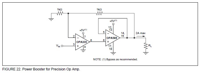
The question is to know if the OPA335 could be replaced by our internal output buffer (Vout_sens connected to the OPA569 directly and Vout to the OPA569 IN+).

I don't see any stability issue, do you?

Could you share more details on the R to R and offset characteristics of our output buffer?

Regards,

  • Hi,

    Stability will be an issue here, since our output buffer has a gain of 2 and the intention of having VSENSE pin coming out is to compensate for any voltage drops while driving long cable.

    Since OPA569 connected to output of the DAC and feedback is taken from the load side, essentially we will be having delay in the feedback network which can cause stability problems. In what gain configuration you are going to use OPA569?

    We need to do stability analysis in simulation to assess how much phase margin we will have after adding OPA569. Let me check with the design team to get the output buffer characteristics and I will do a sim and get back to you.

    What do you mean by R to R here? Rail to Rail? 

    Also you want to know the offset of the DAC right? or specifically for the output buffer?

    Regards,

    AK

  • Hi Akhilesh,

    R to R for rail to rail, correct.

    My point was to understand what kind of accuracy we are able to provide on the output buffer.

    The OPA569 will be used in unity gain.

    I've missed from where the gain of 2 is coming from (I though the buffer wasn't impacted). Can you explain?

    Regards,

  • Hi,

    Please see the simplified diagram of the DAC below.

    Vref is divided by 2 and applied to the string and buffer is in gain of 2.  This is the reason we cannot directly assess the stability of the circuit with OPA569.

    I will get the offset details soon. Please give me a day or so.

    Regards,

    AK

  • Hi,

    Worst case offset for the DAC is +/-5mV.

    Closed loop output impedance of the buffer is in the order of 100milli Ohms and the internal gain is achieved by two 100K resistors.

    You can try to model the output stage with these values to get an idea about stability. Keep in mind that this will be an approximation, since this part is 20 years old, I couldn't run a simulation to get the stability owing to software compatibility issues.

    I suggest moving to newer DAC like DAC80501. 

    https://www.ti.com/product/DAC80501

    Regards,

    AK