This thread has been locked.

If you have a related question, please click the "Ask a related question" button in the top right corner. The newly created question will be automatically linked to this question.

DAC8554: Glitch Energy for Cross Talk

Part Number: DAC8554
Other Parts Discussed in Thread: DAC80504, OPA627,

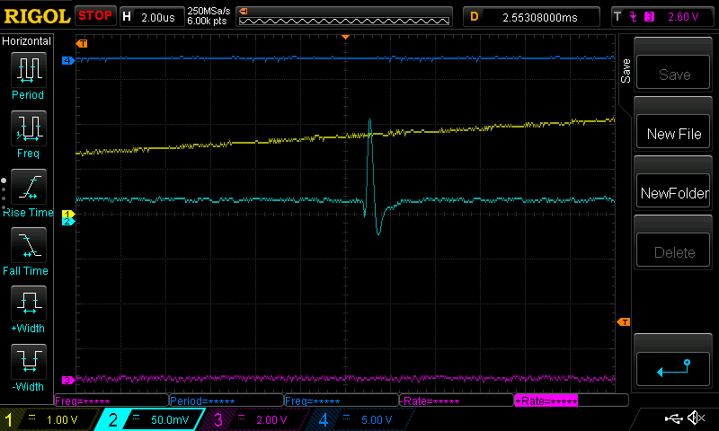
I'm trying to understand the glitch energy on the DAC8554 better as I'm seeing higher than expected glitching and different results on different channels. When trying to recreate figure 35 in the datasheet, I observe that the glitch energy is not a function of LDAC (soft or hard) but happens whenever the data buffer (not DAC register) is updated. Also, I see the same glitch on all channels, regardless of which one is being written to. For example, if I change the data buffer on channel B from 0x7FFF to 0x8000, I see glitch with the same amplitude on channels A, C and D as I see on channel B. Is this expected?

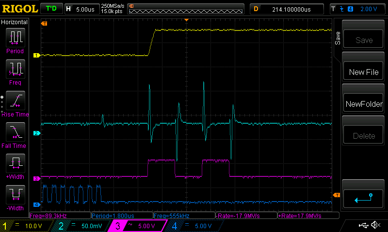
On my circuit, I'm seeing increased glitch energy on some channels. Specifically, when updating channel A data buffer, I see a bigger glitch on channel B. Also, when updating channel C, I see a big glitch on channel C than when updating other channels. Is there any reason to expect different channels to have larger glitches that other channels or be more sensitive to changes in other channels? If this is a layout issue, are there any layout recommendations to reduce glitching? Is all the glitching on the DAC output pins, or are there other pins / radiation (EMI) that contribute that I should be aware of for design and layout?

Thank you,

Ben

  • Hi Ben,

    Do the glitches correspond to the digital edges of your communication? If so, then I expect that you have some digital feedthrough issues. Take a look at these training videos for a good explanation of some of the sources of the digital crosstalk and glitch.

    The best way to reduce feedthrough is to ensure there is a low impedance path to the ground current return point from the power circuit.  This device only has one ground pin, but it does have a VREFL pin.  

    Do you think you could post your layout for review?

    Thanks,

    Paul

  • Thanks for the reply and the videos. I watched them, but I believe my layout follows their recommendations. I'm pretty sure I've ruled out digital coupling as the issue: I slowed down the DAC clock and I when I send DAC commands with no effect (set address select = 2, when hardware address is 0, for example) I see two glitches per command. One glitch is a negative pulse that is 400ns wide and starts exactly 200ns after the SYNC line goes low. The other glitch is positive and happens exactly 200ns after the fall of the 24th SCLK cycle. If this were digital coupling from the SYNC signal, I would expect to see glitching on both the rising and the falling edge. Likewise, SCLK and DIN are ruled out since I don't see noise during all their other transitions. I believe this means that internally the DAC does something when the SYNC going low and after the 24th clock cycle that is causing my circuit to glitch.

    With this setup of sending functionally no-op commands, I (conservatively) measure the glitch energy to be 0.35 nV-s for Channel A, 0.7nV-s for channels B and C and 0.4nV-s for channel D.

    If I jump the DAC output by 200mV (software LDAC) and look at glitching on the other channels, I get the same results as as with the no-op command, except when jumping channel A and looking at glitching on channel B. In this case, I see twice the glitch energy: 1.4nV-s. The glitch energy is not a function of the DAC output jump size, but seems to be related to the DAC code change.

    Finally, I had each channel jump from value 0x7FFF to 0x8000 (again with software LDAC) and looked at the glitches on all the channels. In most cases, I see the same glitching as before. 0.35nV-s for channel A, 0.7nV-s for channels B and C and 0.4nV-s for channel D. But again I see 1.4nV-s glitch on channel B when updating channel A. However, I also see 1.3nV glitch on channel C when updating channel C.

    What can explain this behavior? For some reason Channels B and C are more sensitive to any command updates than channels A and D. Additionally, there does not appear to be significant cross talk from one DAC channel output to another, but there is glitching cross-talk for DAC code changes on some channels. If the output of DAC Channel A does not affect channel B, why does changing the DAC code on Channel A from 0x7FFF to 0x8000 cause a large glitch on channel B? I would expect typical DAC code change glitching to affect all channels equally via an internal glitch in Vref from the load change. It seems like channels B and C have an extra means of noise coupling. For channel B, it is on code changes on channel A and for channel C it is code changes (or DAC changes, it is hard to separate) on the same channel. 

    Below are images of the layout --  the layout uses a single ground plane for analog and digital but there is a virtual split based on component placement. In the DAC8554 is the origin, then digital signals go up and analog signals go down. IOVDD and AVDD are generated from their own voltage regulators and as does the VREFH. VREFL is tied to ground. The layout is basically a single layer design with other layers bringing in power or providing a ground plane.

    Any ideas on what could be going on or tests to try to narrow down the issue would be greatly appreciated. Thank you,

    Ben

  • Hi,

    Your layout looks fine to me with proper analog and digital signal separation.

    Can you please post scope shots of your measurements for the worst channel and good channel with proper trigger ( either LDAC or SYNC for reference)

    Lastly please provide scope shots of your SCLK signal, just want to check signal fidelity.

    One quick thing to check whether its digital coupling or not, you can either reduce IOVDD or reduce speed of your SCLK.

    if its related to digital coupling, you should see proportional change in amplitude.

    Regards,

    AK

  • Thanks for the reply. Attached are some o-scope shots. In this setup I update DAC Channel A from 0x7FFF to 0x8000 with soft LDAC (DB21 = 0 and DB20 = 1). I look at DAC outputs on channels A and B. The DAC outputs on the O-scope have a 5x gain (and 1.6 MHz first-order low pass filter) and are rescaled from 0-4.096V to +/-10.24V. Yellow is DAC Channel A and cyan is DAC Channel B. SCLK is Pink and Blue is the SYNC line.  The picture below has the O-scope average for 256 shots. 

    This is the same setup, but without O-scope averaging.

    Here the channels are the same, but we are zoomed out to see the full 24 cycles of the SCK and the pulse of the SYNC line. First picture is with averaging, the second one without.

    I will look into adjusting IOVDD, but I think that is somewhat involved in my circuit. 

    Thanks for your help,

    Ben

  • Hi,

    I am checking  with my lead designer to look into this in more detail. Meanwhile can you do the other experiment I have suggested, even though I am pretty sure that it has nothing to do with digital coupling. Just want to rule out that variable :)

    Regards,

    AK

  • Hi,

    I had a check with my design team and we concluded that this may be an issue with the internal layout of the device.

    Also  1.4nV-s is a low level glitch when considering the potential for layout coupling effects. Since these are very old parts ( more than 15 yrs), we cannot do much about this at stage.  Also if you look at the glitch energy specifications in the datasheet, only typical value is  written ( 0.15nV-s), so max values can be bit higher than that.

    Hope you understand this now. Sorry for the inconvenience.

    Regards,

    AK

  • Just to confirm, while 0.16nV-s is the typical glitch energy spec'd for the DAC8554, the datasheets shows many DAC code changes with 0.08nV-s or less. In either case, a glitches of 1.4nV-s is nearly 10x the typical spec (and 20x what is shown in the plot for the same DAC code change), which seems way too high above typical to be considered in spec.

    Also, I was able to adjust IOVDD from 3.6V to 4.2V but observed no difference in the glitch energy.

    Thanks,

    Ben

  • Hi Ben,

    Please consider that the VREFL and the GND are sharing a via to the ground plane in your layout.  That is not necessarily the cause of this, but it could definitely contribute as the digital ground currents will now bias the low side of the reference.  You see a nearly similar glitch when the SYNC line goes low or high.  In fact, I would guess that you would see this same glitch if you simply toggled the SYNC pin, and did not issue any commands.  (do you think you could try that and share the results?)

    If possible, let's try an experiment:

    I do not see a schematic on your board, but I assume you are using one and that it has a ground or ground-sense pin.  I want you to use a knife and cut the trace connecting VREFL to the GND pin/via.  I have drawn the line in red.  I would then also like you to use a small wire and bridge the VREFL pin (by using the pad on the capacitor) to the VREF source ground.  I expect that when you do that, you will see the CS line not impact the output as much.  Now, that being said, the wire might result in a higher actually code-to-code glitch.

    Thanks,

    Paul

  • Hi   --

    Thanks for looking at this and the suggestions. That's a good find on the grounds sharing a via. I will definitely fix that in the next revision and discuss how to test that below, but first I wanted to show more data about the SYNC glitching.

    SYNC Glitch

    Previously, I was seeing glitching on SYNC going low, but not high, but your suggestion to just toggle the SYNC line was a good one and when I did that I saw no glitching. Which was inconsistent with what I previously saw. What I found was the glitching depends on the change of the DAC state. Here's the sequence of events:

    Toggle SYNC -> Send 0x7FFF to DACA w/ Soft LDAC -> Toggle SYNC -> Send 0x8000 to DACA w/ Soft LDAC -> Wait -> Repeat

      No Glitch                 Big Glitch                                                Glitch                         Glitch

    Inverting the order inverts the behavior:

    Toggle SYNC -> Send 0x8000 to DACA w/ Soft LDAC -> Toggle SYNC -> Send 0x7FFF to DACA w/ Soft LDAC -> Wait -> Repeat

      Glitch                          Glitch                                                No  Glitch                         Bigger Glitch

    Somehow the state of the DACA affects whether or not there is glitching on DACB when the SYNC line is toggled. This seemed weird, so I did two SYNC pulses in a row and I only see glitching when SYNC goes low the first time it goes low after updating DACA to 0x7FFF. I have no idea why. Below are pictures showing the effect, the first one 0x8000->0x7FFF and the second on the reverse. It isn't super easy to tell, but there is really only one glitch when the SYNC line goes low and it is fully resolved before the second pulse (where there is no glitch).

    Cyan is DAC Channel B output; Pink is  DIN; Yellow is SCLK; Blue is SYNC. 

    VREFL Ground

    I'm not sure I understood your comment "but I assume you are using one and that it has a ground or ground-sense pin" so maybe you could clarify. I am using one ground plane for all grounds (digital, VREFL, analog) and I'm trying to virtually have a split ground plane based on placement between analog and digital grounds. I definitely see the problem with having pin 5 (VREFL) and pin 6 (GND) share a via.

    I'm not entirely sure how to do this yet, but I was wondering your thoughts about cutting the pin 6's trace to that via instead of pin 5's. This way the 'bad' ground connection that I wire up would be on the pin6 ground instead of the VREFL ground pin. My thinking is that the pin5 VREFL pin would be more sensitive to noise and ground shifts, so leave it with the better ground connection. What do you think? Of course if I do that, I don't have a pad to use to solder to pin 6 and I'd also have to lift the 5V cap filtering the 5V line to that same ground via as well, so this might not be very reasonable. But if you think that's a better test / solution, I'll look more carefully about finding a way to do it.

    Also, I'm wondering if you have any thoughts on what could cause this glitching to be asymmetric across channels. I would expect bad VREFL ground connections to cause glitching on all channels equally, not channel B only, and not especially when updating DAC channel A. Or am I missing something about how this issue would couple into the chip?

    Thanks again for all the help,

    Ben

  • Hi Ben,

    I will need some time to review this, but one thing I just want to check very quickly: Can you confirm what state your LDAC pin is in? Any chance that pin is floating?  Does the glitch behavior change dramatically when you use LDAC pin instead of the software LDAC?

  • Hi Paul --

    The LDAC pin is low unless I mention toggling the LDAC pin. With the shots above showing the SYNC pin toggling, if I remove the soft LDAC, I still see the same behavior with SYNC causing a glitch after a (no LDAC) update. However the glitch from updating to 0x8000 goes away and the glitch when going to 0x7FFF gets smaller but is still significant. Roughly it seems that the glitching for LDAC (soft or hard) is about as bad at whatever this other glitching is. (I'm hoping if I fix the first one, maybe the LDAC glitching will get fixed too).  When using the hard LDAC instead of the soft LDAC, I see slightly more glitching, which I attribute to doing an LDAC on all channels instead (with the soft) just the one. But the glitching on the falling of the 24th clock cycle happens with or without a soft (or hard) LDAC.

    Let me know if you have any more questions or if you'd like me to take any data.

    Thanks!

    Ben

  • Paul --

    Sorry if this double posts, my last reply seemed to get lost. 

    In general, the LDAC pin is low. I did some tests with not doing the soft LDAC and using the LDAC pin and it didn't make a big difference. The LDAC pin does produce bigger glitches, but I attribute this to the fact that it does updates on all channels instead of just one. 

    The weird thing I see is I get glitching even when doing no LDAC (hard or soft). In the pictures above with the SYNC pin toggling, if I remove the soft LDAC, the glitch when going to 0x8000 goes away and the glitch going to 0x7FFF gets somewhat smaller, but the SYNC glitch stays the same and the 0x7FFF glitch is still significant. It seems like the glitch from updating the DAC is roughly the same amplitude as the glitch from updating an internal DAC register but not updating the DAC output. I've mostly focused on the latter thinking that is more strange and uses less of the circuitry and thus more likely to be the underlying problem. But in any case, hard vs soft LDAC doesn't seems to have much affect. 

    Please let me know if you have any more questions and if there is some data that would be helpful for me to take.

    Thanks!

    Ben

  • Hi Ben,

    I think we might be seeing some compounded effects of having LDAC low and using the soft LDAC.  Can you confirm what happens if you only use the LDAC pin to update the device? (do not issue a soft LDAC).  Then, can you assert LDAC high and see what happens if you only issue the software LDAC command to update? (you might have already done this test).

    Thanks,

    Paul

  • Paul --

    Thanks for the response. Here's what I did. I set LDAC low and then sent a SPI command to set (without soft LDAC) update DAC Channel A to 0x7FFF and then to 0x8000. Then I pulsed LDAC high and then brought it low again.  For the second test, I did the same with but I had LDAC high initially and pulsed it low. I then looked at glitching on DAC channel B.

    Here are plots for those two setups. The blue is the SYNC, yellow is the SCLK, cyan is DAC B (5x gain). Purple is the LDAC pin. As you can see, there is still glitching on the 24th SCLK edge of the first command and when SYNC goes low for the second command, regardless of the LDAC pin being high or low. There is much larger glitching when the LDAC pin toggles high or low, and I don't know what to make out of that. When it goes high, it is updating all 4 DAC channels, so I'd expect some glitching, but nothing should happen when LDAC goes low.  Thoughts?

    I hope this helpful. Please let me know if you have any questions on the data, or if there is more data to take that would be useful. 

    Thanks,

  • Hi Ben,

    This is very interesting data, though I do not see anything very conclusive in it.  The second plot seems to make the most sense to me, as that falling LDAC edge should actually cause the DAC to update.  

    Are you implementing very fast logic edges? Are you able to adjust the drive strength of the IO pins?

    I wonder what this would look like if you write the same value on both commands, or write an invalid command I.E. only 8bits of data.  If it is repeatable then I suspect this only a digital crosstalk issue with either the board or the device.  

    Can you dry the GND pin modifications I suggested?

    Thanks,

    Paul

  • Paul --

    I do not believe that the glitching is from signal on the LDAC pin simply because pin driver and the PCB layout for the LDAC trace is almost identical to the layout for the SCLK, DIN and SYNC pins and I cannot see any glitching on those pins, so somehow the layout would have to be causing ~100x worse glitching on that trace compared to the other traces.  All those pins are being driven with the lowest drive strength supported by my hardware. I did increase the drive strength on the driver for the LDAC pin by 6x and I saw no change in the glitching. But it is strange that there is glitching on both edges of the LDAC pin.

    I took the same data I took in the last post but I added more LDAC pulses. The glitching looks the same with every LDAC pulse regardless of is there was a DAC update before it (ie if it was loading something new) or not. I believe this is equivalent to sending an invalid command. Below is the O-scope trace of that data and the second figure zooms in a bit on the glitching. The glitch size looks a little smaller for the first LDAC update in the figure, but this is an artifact of the O-scope time scale -- when I zoom in to really see the pulse, all 4 look the same.

    I'm going to cut the ground trace you suggested and see if what that does. Hopefully that data will be interesting / useful. 

    Thanks for all your help,

  • Hi Ben,

    I am very interested in seeing the behavior after changing the ground connects.  There is a possibility of the LDAC having a much higher digital feedthrough due to some layout in the die, but I have not seen that issue before with this device.

    Thanks,
    Paul

  • I ended up not cutting the trace because pin 5 and pin 6 are connected at the cap pad upstream of where you suggested cutting the trace, so I think we'd still have the same issue of the two grounds sharing a single via for the return currents. Instead what I did was I lifted pin 5 on the DAC8554. I stood the Vref cap vertically on the Vref pad and connected the top of the cap to pin 5 and then ran a wire from pin 5 to ground. I believe this achieves what you want: the 5V return current (pin 6) goes to ground through a via that is isolated from anything on the Vref circuit. The Vref has cap filtering directly between pins 3 and 5 and pin 5 goes to ground via a via that is only shared with analog Vref-biasing circuitry. 

    Unfortunately, this made no difference in the glitching as it looks identical to the posts I uploaded previously. 

    I'm running out of ideas. Any thoughts on things to check / test?

    Thanks,

  • Hmmmm... I am also running out of ideas.  Can you try one last test? Can you externally drive LDAC with a very slow edge? For example, use a power supply output with a very low current limit (~1mA).  I am hoping the edge is slow, like <1V/ms.  Does the glitch go away, or is there still a sharp glitch when the LDAC signal crosses the VIL threshold?  This will narrow down if the glitch is caused by some internal mechanism by the LDAC updating, or if the glitch is caused by some parasitic feedthrough.  

    To be fair though, neither of these cases are easily remedied.  If it is some parasitic layout issue within the device, then we are probably stuck with behavior.

    For another point to clarify - does this only exist on one board? Or all your boards (if you have built more than 1)?

    Thanks,

    Paul

  • I was able to drive the LDAC pin with a saw-tooth ramp, so this has a very slow slew rate in one direction. And then I inverted it so the slow rate was on the other transition. In the force cases (low->high fast, low->high slow, high->low fast, high-> slow) I see no noticeable difference in the glitch. I do have multiple boards, so I can test to see if the glitching is the same on multiple boards. I'll let you know what I find.

    In the images below, the yellow trace is the LDAC pin and the cyan is the DAC channel B glitch. 

    Thanks,

  • Paul --

    I tried a brand-new board and I see identical glitching. However, while setting that up, I discovered something interesting. I accidently left the Vref disabled (Vref is generated with a MAX6070 which has an ENABLE pin that I can control). In this situation, Vref is 0V and at least when the circuit is off, Vref has an impedance of 1.5k Ohm to ground. In this situation, I see no glitching at all. When I re-enable VREF, the glitching comes back. But the really surprising part is the time-scale. If I take a board that is glitching and disable VREF, the VREF voltage drops from 4.096V to 0V with an exponential decay and a time constant of ~50ms. But the glitching decreases roughly linearly over about 1 second. This is hard to measure quantitatively since I cannot see the glitching when the O-scope is configured for long time-scales, but after ~100ms, VREF is basically at 0V but the glitching is about 75% of its original strength. Half a second after disabling the VREF, Vref is definitely at 0V, and the glitching is at 1/2 or 1/3 of its original value. After about a second, the glitching is too small to measure.

    Any ideas what this means? Anything I should be looking more carefully at? I do not see any glitching on the 4.096 Vref line. 

    Thanks,

    Ben

  • Hi Ben,

    This is interesting behavior as it probably means the crosstalk is coming in through the reference structure (though it still may be internal to the device rather than external).

    To clarify, let's say you set the DAC output to 3 different values and toggle the LDAC to see if the magnitude changes (0xFFFF, 0x8000, 0x0000 or full-scale, mid-scale, and zero-scale).  Does the glitch magnitude change?  If it does not, then maybe we have issues with the VREFL input ( the one that is partially shared with ground)  If it does change, then we probably have internal crosstalk.

    Thanks,

    Paul

  • Paul -- 

    I can't say I understand anything better, but I have more data. 

    First, I disabled the Vref regulator and connected Vref to an external power supply. If I turn the power supply off, the glitching goes away (well almost, but at least 10x better). If I turn on Vref power supply to even 100mV, the glitching comes back at almost full strength. So it is very weakly a function of the Vref voltage, but mostly seems to need a stiff power supply. I tried adding 3 Ohms in series to the power supply providing Vref signal to make the source less stiff but that had no effect.

    As a reminder, when doing a single-channel update (soft LDAC), the biggest glitching I see if on DAC B when I update DAC A. When doing a hard LDAC, the glitching is 2-5x times worse. (The variation is because the soft LDAC glitching is a function of the DAC code and the hard LDAC seems not to be). 

    I updated the DAC A from 0 to 0x8000 to 0xFFFF and did 2 hard LDAC pulses after each update while monitoring DAC B. A plot of that is below with DAC A in yellow (5x gain) , DAC B in cyan (5x gain) SCLK in magneta and LDAC pin in dark blue. The glitching is the same for every LDAC pulse regardless of the DAC code or if it was the first or second LDAC pulse. 

    Here are zoom-ins on each pulse:

    I also tried removing the hard LDAC pulse and doing a soft one-channel LDAC (update DAC A, look at DAC b). In this setup, the glitching was worse when updating from 0x8000 to 0xFFFF while the other two updates (0xFFFF->0x0000 and 0x0000->0x8000) were about half as much. There was also a glitch the same size as the smaller ones when the SYNC line when low at the beginning of the 0x0000 transaction (but no other transactions). 

    Any ideas? This all just seems so weird.

    Thanks,

  • Hi Ben,

    This is not making much sense, but it is making me think there is some weird glitch behavior in the device itself.  Were you able to try my "very slow LDAC edge" experiment?  If a very slow edge results in a similar glitch, then we know it is some digital latching behavior inside the device. 

    Otherwise, I am pretty much out of ideas, and I think it would be more productive to investigate ways to reduce the glitch's impact on the rest of your system or move you to another device with better glitch behavior (DAC80504).

    Thanks,
    Paul

  • Hi Paul --

    For the slow LDAC edge, please see my post on Nov 18, 2020 6:53 PM -- I put a sawtooth triangle wave with a very slow slew rate on LDAC and it made no difference.  

    This is maybe a strange question, but is it possible this could be an issue with an counterfeit device? (Are there such things for this part?) I would like to think that my assembly house would source parts from reputable vendors, but this behavior is very strange so I thought I'd ask.

    The DAC80504 is 2x the cost and major redesign, so I don't want to go that route unless absolutely necessary. Also if I'm seeing 20x the glitch than expected with the DAC8554 (and I do not understand why), I worry that a new chip with also have the same issue.

    Reading the datasheet of the DAC80504, I have a few questions. 1)  it has one glitch type as being 4nV-s which seems very high:  "Code change glitch impulse 1 LSB change around major carrier 4 nV-s". I don't understand what  'around major carrier' means, but it sounds like a glitch when you change by just one LSB and that this glitch would dominate the other spec'd glitches. Also, the DAC8554 does not seem to spec that type of glitch, but should I expect similar behavior?

    Also, in the datasheet for the DAC80504, figure 45 is very interesting. The text says that it is cross-talk glitch when changing other DAC channels, but the glitch occurs when the CS line goes low, meaning at the very start of a SPI packet before any data has be transferred. I see the exact same glitch in my system -- I get one glitch on the 24th edge of the SCK (when the SPI packet is read which makes sense) and one when CS goes low (for the first time after an update) which doesn't make sense to me. Does this means this is expected behavior? 

    On a different note, I didn't mentioned this before, but I have a different power supply powering IOVDD (3.6V) and AVDD (5V). I thought this voltage difference might matter since all the data on the DAC8554 has them at the same voltage, so I raised IOVDD to 4.5V but it made no difference in the glitching. 

    Thanks,

  • Hi Ben,

    Sorry for missing that post.  That certainly makes me think this some kind of internal feedthrough or parasitic resistance path to GND.

    It is hard for me to say if this could be a counterfeit part.  I have certainly seen counterfeit issues before, but generally they very popular devices.  This device is fairly popular, but really hard to say for sure by reaching out to the distributor.  We always recommend that components get purchased from an authorized distributor.  If you can provide all of the markings on the device, I can at least confirm if the markings make sense, but I am not allowed to comment on authenticity on the e2e forums.  It can only be verified by starting a "quality return event", but that should be coordinated by you and the distributor that sold the devices.

    In regard to the DAC80504, that is my mistake.  I was thinking that the DAC8554 was an R-2R DAC, but it is a string DACs.  String DACs generally have lower glitch than R2R DACs, but linearity is harder to achieve.  R2R DAC's glitch is also code dependent and is generally the worst case when the most number of bits are changing.  The major carry would be the case with the MSB changes, so generally, code 0x7FFF changing to 0x8000 is the worst case as every bit is changing.

    In that plot, I actually suspect that it is a typo and they mean to label that as an LDAC signal. I can check, though I think this device is not a good fit after all.

    I do not think the IOVDD supply would be causing any issue.

    Can I suggest one more thing? How about I sample the DAC8554 EVM board to you and you can try connecting your digital signals to the board to see if you see similar behavior? I would normally offer to test this in my lab, but due to some covid restrictions, I will unable to assist with that for a few weeks.  

    If you would like to receive that board, please provide this information to me at frost@ti.com.  

    Customer Company Name


    Customer First Name


    Customer Last Name


    Customer Address


    Customer Address in Chinese (if based in China)


    Customer City


    ZIP or Postal Code


    Country


    State or Province


    Customer Phone Number


    Customer Email


    Thanks,

    Paul

  • Paul --

    Thanks for the eval kit. Short version is that I was able to reproduce my issues with the Eval board so I think these issues are related to the DAC8554 part itself. 

    Here's the test I did. First, I removed the C12 so the U2 buffer would not have limited bandwidth and I connected JMP5 and JMP6 so U2 had a gain of 3. I then used J4 to connect U2's pin 3 (plus pin to the op-amp) to either then Channel A or Channel B output. Everything else I left in the default configuration.

    Then I connected SYNC, SCK and DIN from my board to the eval board. I then looped a SPI command to update channel X to 0x7FFF. Either with a soft LDAC or without. 

    On Channel A, I see the same glitching regardless of what channel is updated or if there is a soft LDAC or not. Then is the same behavior I see on my board and this glitch is relatively small. 

    On Channel B, I see the twice the amount of glitching regardless of what channel is updated or if there is a soft LDAC or not. Except when updating channel A with soft LDAC. In this case I see ~4x the glitching. Which again is roughly the same behavior I see on my board. (The bandwidth for seeing the glitch is lower on my system than on the eval board so I'm not comparing the amplitude of the glitches directly).

    Here are some plots of the data:

    DACA (Good Channel) glitch is ~20mV for ~200ns. Same behavior for any updates on any channel. That's roughly a 2nV-S glitch on the O-scope or 0.7nV-s before the 3x gain block. 

    DACB (Bad channel) when updating any channel other than Channel A. ~40mV glitch for 200ns.

    Finally, DACB when updating Channel A. No longer a single glitch pulse, but amplitude is ~130mV. This is a glitch of at least 4nV-s at the DAC output.

    Since the glitching is aligned with only the SCLK edge, I put a 50 Ohm resistor in series on SCLK to slow down the slew rate, but this made no difference. I also tried powering the Eval unit for both external power supplies and the power supplies used on my board, but no combo made any difference.

    Unless you can think of anything else, I'm pretty sure this means the issue is internal to the DAC8554. Since I see the same basic behavior on the Eval Board, I think this rules out something with the reference voltage or the layout on my board, or a counterfeit part. The only commonality between my board and eval board is the digital signals and with the slew rate tests from the 50 Ohms and previously, I don't think that explains what I'm seeing. 

    Please let me know if you think I missed anything or if you have any suggestions on how to improve the performance (or another part to consider switching to).

    Thanks again for all your help and for the eval unit.

  • Ok, I found one more interesting thing. 

    With the Eval board, if I reduce the reference voltage below 3.0V, the glitching goes away almost completely. From 3.0V to 3.4V the glitching increases quickly and by 3.4V the glitching is at full strength where it holds up to 5V. I've found this to be the case both using R15 to adjust the internal reference (U14 output) and when using an external power supply as a voltage reference.

    But when I do the same thing with my board, the glitching stays constant all the way down to 0.2V for the reference.

    The only difference I can see between my board and the eval board in terms of the reference (in both I've used an external power supply as the voltage reference) is that my board has a lot of capacitor filtering (10's of uF across multiple capacitors) on the Vref line whereas the eval board has no cap filtering. Could this somehow be relevant?

    So, I'm completely confused, but getting the glitching to go away on the eval board seems like progress. Any thoughts or theories appreciated.

    Thanks,

  • Quick question, are you providing +15V for the VCC supply on the EVM board? Did you happen to supply VCC with +5V? If that was the case, it possible that the impulse response of the reference buffer is limited, which might be why it looks better with the lower reference voltage (as the amp would have more headroom).

    One thing that continues to confuse me is that we are seeing two-lobe glitch.  This device is a string DAC, so it should have only one glitch.

  • Paul --

    I provided +15V for VCC to the board, along with +5V for 5VA and +3.6V for VDD.

    A couple thoughts about the glitch. I don't think the glitch I'm seeing is the expected string DAC glitch impulse. For one thing, I see it when going from 0x7FFF to 0x7FFF and my understanding is that since no bits are actually changing, this shouldn't cause a glitch. Additionally, the fact that the glitch amplitude depends on both the channel observed and the channel being updated says it is more complicated than the expected code transition glitch. Since what I'm seeing is far greater than the spec'd glitch impulse so it seems reasonable that there is some unexpected glitching in addition to the code transition glitch. In terms of the double lobes I don't know if that is significant, with the eval unit, the DAC has no filtering but since the oscillation frequency is ~3 MHz it wouldn't take much filtering to hide the ringing and just see a more typical glitch. 

    I'm not sure if this is relevant, but I was looking at the datasheet for the LTC2758 (sorry it is a competitor part) and I don't know the part is a string DAC or not, but it spec's 5x worse glitch impulse when powered with 5V compared to 3V (see figures on page 7 and table on page 3). This is much more of an increase in glitching than even a V^2 dependence would predict and makes me wonder if there is something about going above 3V that greatly affects glitching somehow. 

    Still very confusing. Thanks for all the help,


  • Ok, I think I can summarize everything I'm seeing. My previous observation that the glitching depended on the Vref voltage was wrong. With the Eval board, I had the OPA627 negative rail at ground and that hides the true glitching when the signal gets under 3V from the negative rail (0V). When I put in a negative rail (-15V) this effect went away.

    Glitch Summary

    • Intrinsic to the DAC8554
    • Glitching proportional to AVDD
    • Only present when updating DACA and observing DACB or updating DACC and observing DACC.
    • Glitch is 2 nV*s

    Steps to Reproduce

    Start with DAC8554EVM. Modify it as follows:

    • Remove C12
    • Change R8 to 1kΩ (from 10kΩ)
    • Change R7 to 500Ω (from 10kΩ)
    • Change R9 to 500Ω (from 10kΩ)

    Jumper across JMP6 and JMP5. These changes will give U2 a bandwidth of ~3 MHz and a gain of 5.

    Connect +15V to VCC, +5V to +5VA, and -15V to VSS, and VDD to proper digital level. Set JMP10 to short pins 1 and 2. JMP7 to connect pins 1 and 2. Configure reference however you desire. Connect Din, SCLK and SYNC for SPI communication.

    Set all channels to 0x7FFF with SPI commands:

    • 0x107FFF (Update DACA)
    • 0x127FFF (Update DACB)
    • 0x147FFF (Update DACC)
    • 0x167FFF (Update DACD)

    Now in loop, send 0x107FFF (update DACA) and connect U2 +IN pin to OUTB and observe U2_OUT and you will see glitch on the 24th CLK cycle. Glitch will not be there when observing any other DAC channels. When updating DACC, glitch will only be on DACC channel.

    Data

    Blue is DACB while update DACA. Each SCLK transition causes some fast glitching that is mostly symmetric. The SYNC line (yellow) also produces a large ring on its transitions. However, the biggest glitch that does not integrate away is at the center of the trace and 100mV tall and 200nS wide (10nV-s glitch energy with 5x gain from op-amp or  2nV-s energy from DAC).


     Here is the same shot, but observing DACD instead:


    I have observed with with both my custom board and with the DAC8554EVM evaluation board. This, I believe, rules out layout issues or ground connections or filtering of the Vref, etc. I can recreate this when using either an FPGA to send the SPI commands or an independently designed micro-controller. I believe this rules out digital drive strength and the such. My conclusion is this behavior is intrinsic to the ADC8554. I have also adjusted Vref and IOVDD and ADVDD to see if that have any affect on the glitch. Only AVDD affects the glitch size, and it does so linearly. 

    I believe the only work-around is to only use DAC channels A and D. 

  • Hi Ben,

    This is an awesome summary.  I am going to mark your last post as the "resolution", so that future readers know to look to that post.  I am working with our designers to see if they can identify the exact weakness.

    Thanks,

    Paul

  • Sounds good. I'll be interested to hear what the designers say. Thanks for all the help.