This thread has been locked.

If you have a related question, please click the "Ask a related question" button in the top right corner. The newly created question will be automatically linked to this question.

ADS8363: full differential input schematics review

Part Number: ADS8363
Other Parts Discussed in Thread: THS4561, THS4531,

Hi team,

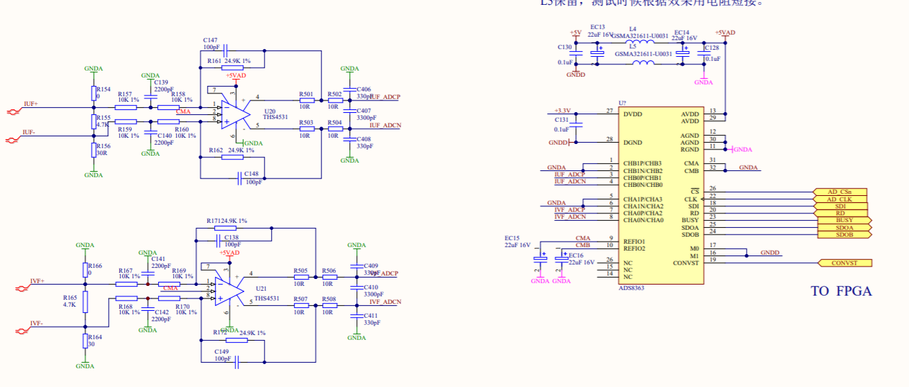
This is my customer design. Could you pls help give any comments? Below are what I found,

1. Leave CMA/CMB pins open, as it is as full differential input use case;

2. Demount R154 R155 R156 C139 C140 C147 C148 C406 C408;

3. For a 16bits application, choose THS4561 with smaller offset;

4. The input signal to FDA is 2.5V common voltage with +-2V swing. Gain is 1.25V/V to differential +-2.5V output swing to ADS8363. I would like to set OCM of THS4531 as 2.5Vref of ADS8363. FDA can be powered by 5V single supply.

This is a two channel simultaneous sampling. Can I use REFIO1 to supply both ADCs and OCMs of amplifier? I think the buffered REFIO1 can do this and single reference introduces higher accuracy.

BTW, I didn't find the ENOB data in datasheet.

Thanks.

  • Hi Jerry,

    The unused inputs on the ADS8363 should be grounded.  Please consider replacing L5 with a direct short or 0 ohm resistor.  You have M0=0 and M1=1 (Mode II) and you show SDOB going to the FPGA.  SDOB is only active when M1=0 (modes I and III), so please verify desired operation.  I highly suggest routing BUSY to an unused GPIO or at least a test point - this makes any future debugging a little easier.

    I'm fine with the removal (or DNI) of R154-156 and R164-166, but keep placeholders for the input caps to U20/21.  Also consider keeping the footprints there for the input CM filter to the ADS8363.  Depending on you desired sampling rate, you may find you need these to get the input settled properly.  You could use one reference for both channels.

    ENOB can be calculated from SNR and THD - it would be ~15.1 bits.

  • Thanks, Tom.

    1. Customer will short L5;

    2. They also grounded unused pins including CMA/B. Yet, NC pins are left float;

    3. Input channels are change to CHA0 and CHB0, as it is as easy as default setting. And, SDI can be simply pulled low for reading;

    4. M0=M1=0, and customer will use full clock mode to get the fast speed.

    Could you pls help take a look the schematics again? Thanks.

  • Hi Jerry,

    Looking better!  Full Clock mode cannot be used with SDI held at '0'.  You would need to program bit 7 in the configuration register to '1' in order to use full clock mode.  There is really no difference in throughput though - FC mode uses 2x the SCLK speed and reads data out in the same conversion cycle.  HC mode uses a slower clock, but outputs sample N while sample N+1 is converting.  The overall throughput is the same.

  • Thank you, Tom.

    I certainly will set bit 7 =1 for full clock mode. This is a motor drive application sampling 2 channels phase current with Simultaneous Sampling. I prefer full clock to make conversion and transmission phases within the same CONVST/RD signal cycle.