This thread has been locked.

If you have a related question, please click the "Ask a related question" button in the top right corner. The newly created question will be automatically linked to this question.

ADS8339: Reference Driver Circuit expressions

Part Number: ADS8339
Other Parts Discussed in Thread: OPA333, OPA388, THS4281, OPA350, REF5045, DAC8552, TINA-TI

Hi everyone,

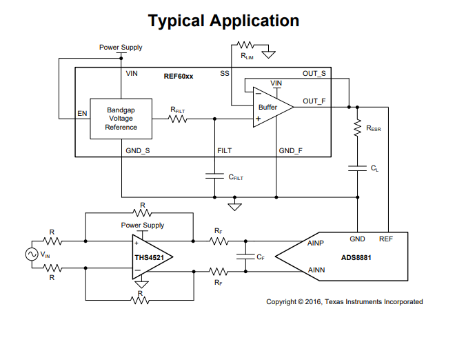
I'm currently working on an ECG acquisition test-bed for analog front-ends. The ADC of choice was the ADS8339 to sample the ECG AFE's output voltage.

I'm thinking about incorporating the reference driver circuit suggested in the datasheet, but I can't find the circuit expressions.

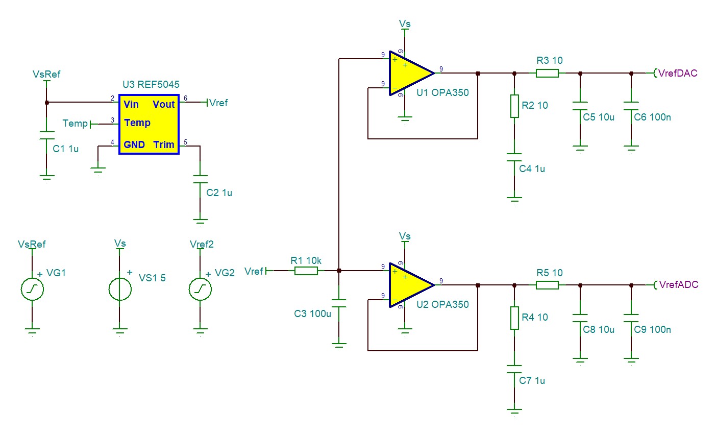
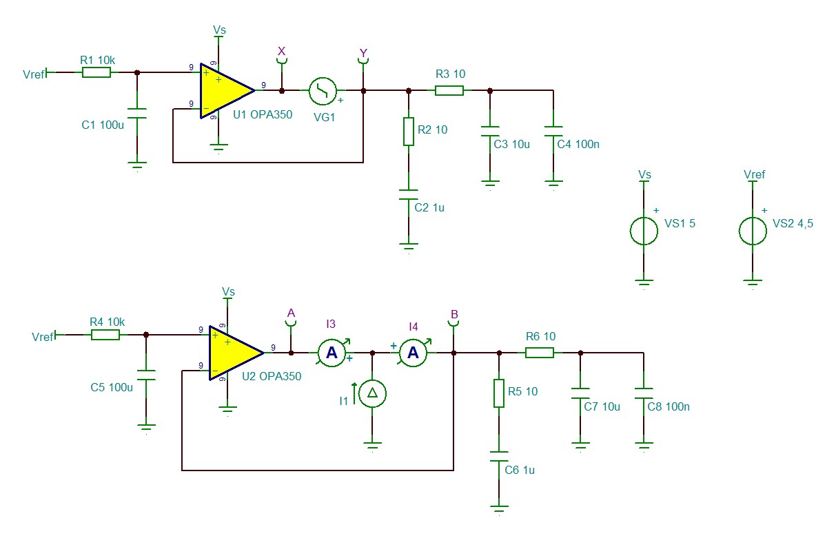
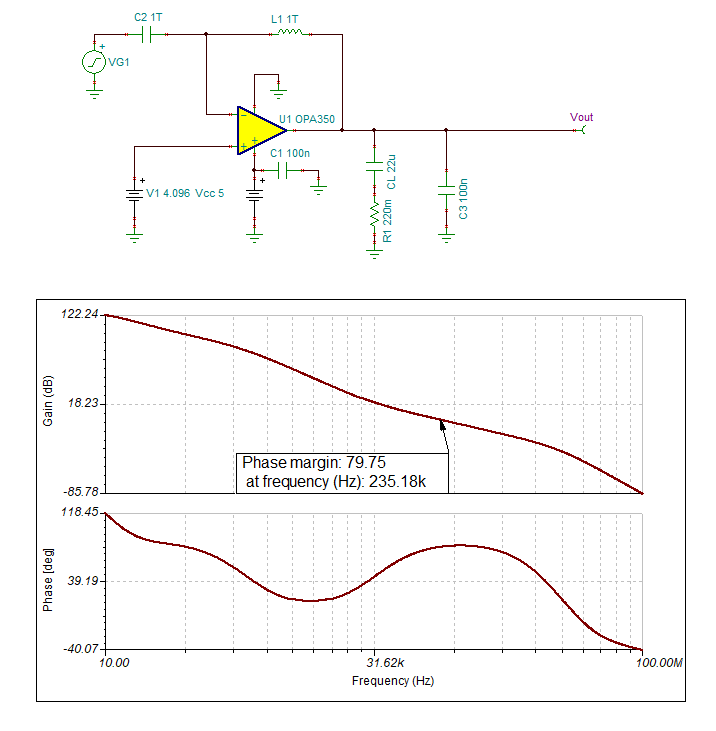
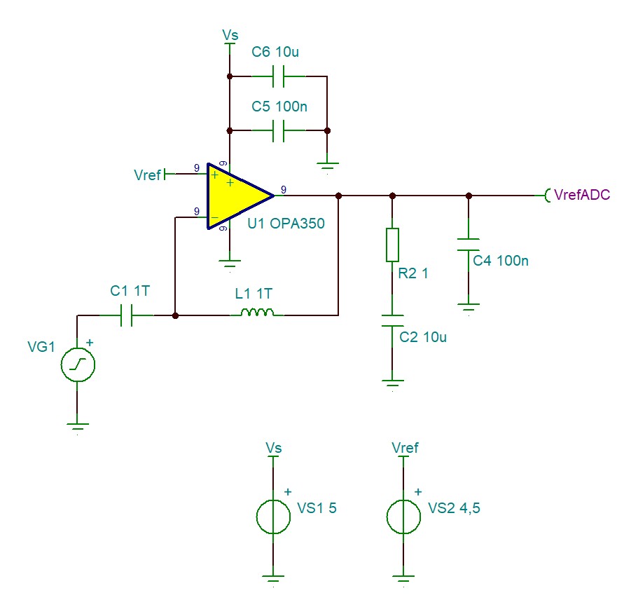
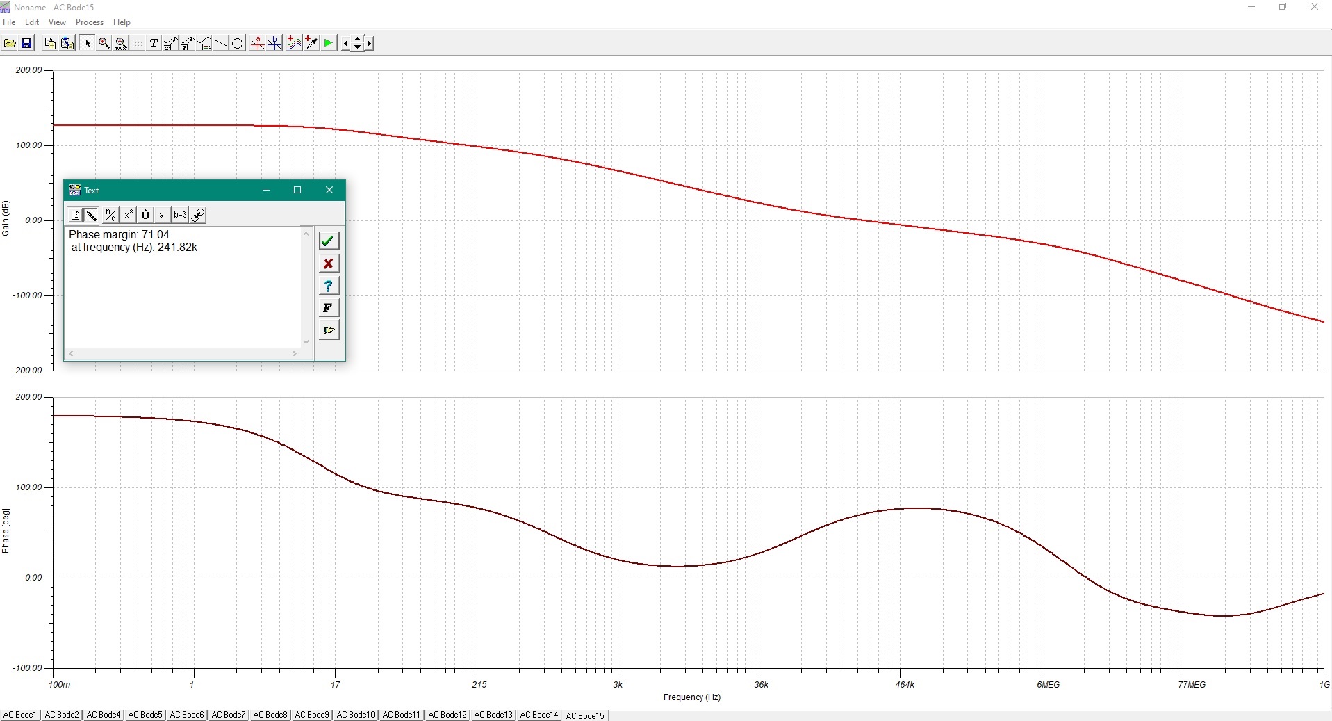
I don't really understand the behaviour of the circuit. PSpice AC simulations reveal that the circuit behaves as a low-pass filter with low-Q.

Circuit expressions that I've taken using KCL show that the circuit has three poles and one zero, if I'm not wrong in calculations or missing something.

The circuit also reminds me of a non-inverting integrator/DC servo, but I'm not sure if it exhibits this behaviour.

Can you help with circuit expressions? I need to know how the circuit behaves, its cut-off frequency, Q-factor and if applicable, the integrator time constants.

As the application is ECG the cut-off frequency must be lower (than 1 Hz) than its current value (of about 17 Hz).

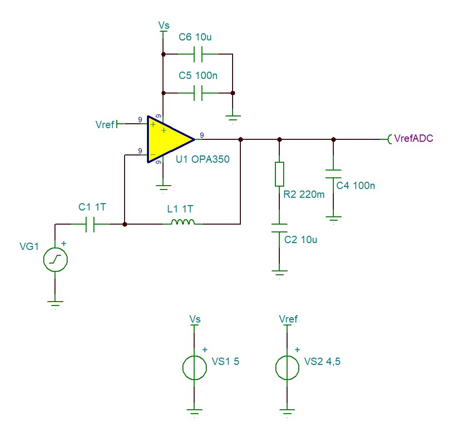
Is it ok to replace the OPA333 with an OPA388 and the THS4281 with an OPA350?

What about exchanging the 1kOhm resistor for a 10kOhm resistor?

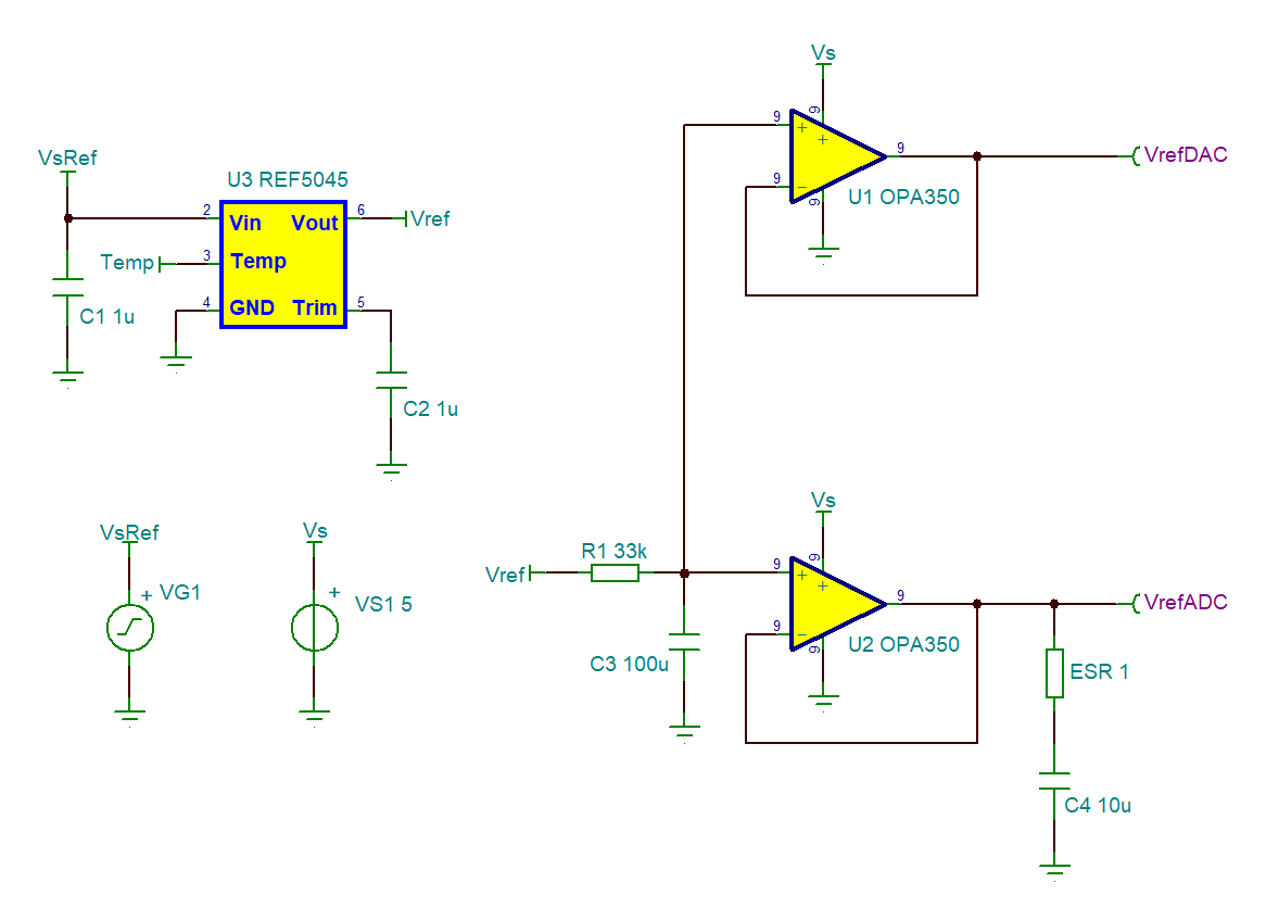
Circuit schematic from datasheet attached.

PS:

Message for the forum administrator/reviewer

I've posted (or tried to post) a similar thread before, please delete the previous thread if not approved.

Kind regards,

Daniel Almeida

  • Hello Daniel,

    The reference input on the ADS8339 is a switched capacitor, and requires fast dynamic currents to recharge during the conversion process.  This requires not only a large charge reservoir (10uF cap), but also a high bandwidth amplifier to resupply this current.  Most high speed amplifiers can meet this requirement, but they usually do not have good DC specifications.  In this case, we use a composite amplifier topology, with a low speed, low offset amplifier (OPA333) providing the DC precision, and the high speed amplifier (THS4281) providing the high speed dynamic charge.

    From a noise perspective, you can view this as a simple RC filter (10k, 1uF) to filter the reference noise, and the composite amplifier simply provides a gain=1 buffer, to drive the ADC input.

    The REF60xx is a new family of references that include the internal buffer, and can directly drive the reference input.  This is usually the preferred approach, reducing the board complexity and component count.

    https://www.ti.com/product/REF6045

    If interested in more details on the composite reference buffer, take a look at this reference design.

    https://www.ti.com/tool/TIPD112

    https://www.ti.com/lit/ug/tidu012c/tidu012c.pdf

    Regards,

    Keith Nicholas
    Precision ADC Applications

  • Hello Keith,

    Thank you very much for your help.

    I currently have OPA350 operational amplifiers, and I will soon order some OPA388s,  in order to reduce project costs this solution seems preferable, I already have REF5045.

    Is it acceptable to use the same reference driver for the ADS8339 and the DAC8552? With individual 10uF||0.1uF capacitor at each input?

    Kind regards,

    Daniel Almeida

  • Hi Daniel,

    The OPA350 and OPA388 should work well, but will probably require some adjustment of the RC values for good loop response.

    The DAC8552 reference input will be easier to drive since it is a switched resistor network, so the same buffer will work.  The reference input pin on the ADS8339 will generate quite a bit of noise due to the switched capacitor.  This pin should have a dedicated reference buffer, and should not be directly connected to any other data converters to avoid noise coupling.

    Regards,
    Keith

  • Hi Keith,

    Thank you very much for your help.

    Which of these alternatives offer the best noise performance? All options consider 10 uF||100nF near the DAC input pin.

    - REF5045 directly driving the DAC reference input pin

    - REF5045 connected to the input of a voltage buffer opamp driving the DAC reference input pin

    - First order active  low-pass RC filter connected to REF5045 implemented with one operational amplifier driving the DAC reference

    - Second order Sallen-Key low-pass filter, Butterworth, filtering REF5045, providing the DAC's reference voltage

    For ADS8339, the suggested reference driver, seems adequate, maybe I would like to lower its cut-off frequency. I need to run some more simulations to check stability.

    With all resistors set at 10 kOhm, and all capacitors set at 1 uF, the Q factor is high, and peaking appears before the roll-off, simulation shows the circuit is stable though.

    The same REF5045 IC may be used for both converters if they have separate buffers. Right?

    Notes:

    I'm replacing the suggested opamps with OPA388 + OPA350.

    The snubber circuit's (Zobel network) component values were modified to 2.2 uF + 10 Ohm, to improve stability. 

    Kind regards,

    Daniel Almeida

  • Hello Daniel,

    The REF5045 may be able to directly drive the ADS8339 reference input, especially at lower sample rates.  We have not tested this, but you may want to add a 0ohm jumper option when you design your board to test this option.

    For lowest noise performance, you can add a single pole RC filter at a very low cutoff frequency to the output of the REF5045.  This will reduce the noise from the reference and provide best performance.  In this case, you will then need to use a reference buffer. However, I think this is probably the best option since you need the reference for both the ADC and DAC.

    Yes, you can use a single REF5045 with two buffers, one for the DAC and one for the ADC in this case.

    Also, if you can tolerate the offset voltage of the OPA350 (this will effect gain accuracy in both the DAC and ADC), then you could just use the OPA350 in a simple buffer configuration, driving a 10uF to 22uF output cap with series resistance of 0.22ohm (needed for stability).

    Regards,
    Keith

  • Hello Keith,

    Thank you very much for your help.

    I will follow your suggestion and combine a first-order filter at the output of the reference with separate buffers for ADC and DAC ICs. Which opamp would perform better as buffer, the OPA388 with lower noise, offset and drift, or the OPA350, with higher bandwidth and output current?

    Best Regards,

    Daniel

  • Hi Daniel,

    If you want to use a single amplifier as a buffer, then you will need to use the OPA350 to drive the reference input of the ADS8339.  The OPA388 can not directly drive the switched capacitor load and show good results.  If the DC specifications of the OPA350 are not good enough (will result in additional gain error in the ADC), then you can use the composite amplifier approach with the OPA388 providing the DC accuracy, and the OPA350 driving the load.

    Regards,

    Keith

  • Hi Keith,

    Thanks for your help,

    I've run some simulations to check the phase margin, and I had to change the RC snubber values to 10 Ohm + 1 nF. I also added a 10 Ohm resistor in series with the output, I'm not sure if the 10 uF||0.1uF are mandatory at the reference pins of the converters (ADC and DAC), since there is a buffer driver and an RC filter before it.

    Simulation shows a phase margin well over 70 degrees, and no evident peaking.

    Could you provide me information about input pin impedance of both devices? DAC8552 reference input impedance can be modeled by a resistor (from the resistor string)? As about the ADS8339 input impedance I really have no idea, is it possible for you to provide me an RC value, of course if it is not confidential information. I want to be sure the circuit will not oscillate.

    Keith Nicholas said:

    Hi Daniel,

    If you want to use a single amplifier as a buffer, then you will need to use the OPA350 to drive the reference input of the ADS8339.  The OPA388 can not directly drive the switched capacitor load and show good results.  If the DC specifications of the OPA350 are not good enough (will result in additional gain error in the ADC), then you can use the composite amplifier approach with the OPA388 providing the DC accuracy, and the OPA350 driving the load.

    Regards,

    Keith

    I think the OPA350 has good performance in this regard as mentioned in www.ti.com/.../tidu012c.pdf, the composite amplifier would perform better, but will require a larger component count and increase system complexity a bit.

    PS:

    I'm measuring gain and phase margins using the technique described by Middlebrook, R.D., in "Measurement of Loop Gain in Feedback Systems", Int. J. Electronics, vol 38, No. 4, pp. 485-512, 1975.

    I'm not sure if it's the most accurate technique, but was the only one that worked in TINA, it requires the post-processor, introduction of the expression ((I3(s)/I4(s))*(-X(s)/Y(s))-1)/((I3(s)/I4(s))+(-X(s)/Y(s))+2) in line edit, creation and insertion of a new curve after running AC analysis, only VG1 must be defined as input and X and Y pins must be defined as outputs.

    I'm using the macro models from

    the model included in TINA is not very accurate in terms of noise and AC performance.

    Converter Noise Filter - stability.TSC

    Converter Noise Filter.TSC

    Thank you for your attention

    Best regards,

    Daniel

  • Hi Daniel,

    The input of the ADS8339 reference pin is a switched capacitor approximately equal to 1/4 of the input capacitance, or 15pF.  The average input current depends on the sampling rate, and is specified as 75uA when running at 250ksps with a 4V reference.  This current will scale linearly with sampling rate; at 50ksps the average current will be closer to 15uA.

    This current will create a voltage drop across the 10ohm series resistor.  At 250ksps, this will be around 750uV, creating a gain error.

    You can use 22uF capacitor with 0.22ohm series resistor and still get around 80deg of phase margin.  This will also eliminate the gain error.

    The DAC8552 is a resistor string, and the input resistance is specified as 62kOhm.  There will be small glitches, and a similar input buffer should easily drive this input.

    For more information on stability analysis and how to use TINA-TI, please take a look at TI Precision Labs- Op amps, section 10.3.

    https://training.ti.com/ti-precision-labs-op-amps

    https://training.ti.com/ti-precision-labs-op-amps-stability-spice-simulation

    Regards,
    Keith

  • Hi Keith,

    Thank you very much for your help. That method for stability assessment is much easier and simpler.

    Does the driver's output/ADC's input require a capacitance to be present? In the schematic you've attached capacitor C3 is at the output, is it necessary in the circuit or was it only used to demonstrate operational amplifier stability while driving (large) capacitive loads?

    The DAC8552 can be directly driven without filtering capacitance, right? Given it is a resistor string. The glitches you mentioned are related to switching between divider outputs? Does the driver for the DAC requires a snubber circuit too? It's input does not present significant capacitance, right?

    Best regards,

    Daniel Almeida

  • Hi Daniel,

    You do not need the additional 0.1uF cap, C3, if the primary capacitor, Cl(22uF) can be placed directly next to the ADC, at the reference pin.  The circuit is stable with this additional capacitor, and helps with the fast load transients created by the switched capacitor reference pin.

    Take a look at the DAC8552EVM user's guide.  The reference pin is directly driven by the output of a buffer with no capacitance, so you can get good results without an additional capacitor.

    https://www.ti.com/lit/ug/slau172a/slau172a.pdf

    Regards,
    Keith

  • I appreciate your help. I think the 100 nF capacitor doesn't introduce much phase shift at the output and might actually show better behaviour at higher frequencies, so it's ok to include it.

    I've run a few simulations in TINA to assess reference driver stability using the OPA350. Currently there are no non-polarized (non-electrolytic) capacitors with more than 2.2 uF at my university's stock, and I'm also not sure about resistors under 1 Ohm. If we order only passive components we are adding much cost to the project, due to expedition and handling costs which are about 10 times higher than the components itself.

    I don't know if I can replace the 22 uF with a 2.2 uF non-polarized (polyester), and a 1 Ohm resistor instead of the 220mOhm. Or is it better to use an electrolytic capacitor with 10 uF in series with a 1 Ohm resistor? 

    Since the circuit is for an ECG application, the sampling frequency of the ADC is set at 1 kHz.

    ADS8339 reference driver (v3) - C2 is polyester, C4 is ceramic.

    Phase margin is over 55 degress for driver v3.

    ADS8339 reference driver (v4) - C2 is electrolytic, C4 is ceramic.

    Phase margin is over 57 degrees for driver v4.

    ADS8339 reference driver (v5) - C2 is polyester, C4 is ceramic.

    Phase margin is about 71 degrees for driver v5. Stability is assured.

    Converter Noise Filter - stability (v3).TSC

    Converter Noise Filter - stability (v4).TSC

    Converter Noise Filter - stability (v5).TSC

    Of course the best solution is the v5 circuit, the problem are the added costs, are v3 or v4 acceptable options? If so which one is better?

    PS: The 0.22Ohm resistor even if not in stock, can be purchased in a retail store, it's cost should be minimal. The capacitor is much more complicated, retail stores only sell electrolytics over 10 uF, I might be able to get a 10uF polyester capacitor at an acceptable price, is it suitable for the application? A possibility would be 10 uF (polyester) + 0.22 Ohm in parallel with 0.1 nF (ceramic), driver v5, is it an acceptable solution? Electrolytic capacitors in my opinion are not very good for higher frequencies and may degrade the circuit's response, and decrease the phase margin. At local stores and at my university's stock, ceramic capacitors are available up to about 1 uF (maximum) and polyester up to about 10 uF (maximum), above those values all capacitors are polarized electrolytic.

    Best regards,

    Daniel Almeida

  • Hi Daniel,

    You can use an electrolytic capacitor and will not need to add an additional series resistor.  These are only needed for low ESR ceramic capacitors.  Just check the datasheet for the capacitor and confirm the ESR is in the range of 0.25ohm to 1ohm for best performance.  You can then simulate to confirm phase margin based on the ESR spec.

    Also, since you are only running at 1ksps, you can directly drive the ADC input with the REF5045.  The buffer is needed to support the higher data rates.  The internal REF5045 buffer and support around 100ksps at 16b.

    It is important to use a larger capacitor to supply the reference load current.  You can try using a 2.2uF, but I think you will see higher noise as a result.

    Regards,
    Keith

  • Hi Keith,

    Thank you very much for clarifying my questions.

    I need two reference drivers, one for the DAC and another for the ADC, the DAC driver is necessary because of the RC low-pass filter, this driver doesn't require a capacitor at it's output.

    The ADC reference driver has a low-ESR aluminium electrolitic capacitor at it's output, the resistance values are between about 0.1 and 1.5 Ohm. I've decided to remove the 100 nF capacitor from the output because it would cause instability if for some reason the ESR is higher. The simulation shows the circuit is stable, with a phase margin over 86 degrees for an ESR of 1 Ohm. 

    Do you consider this circuit adequate?

    Converter Noise Filter (v6).TSC

    Best regards,

    Daniel

  • Hi Daniel,

    This circuit should work well with one exception.  The output of the REF5045 requires an output capacitor connected directly from pin 6 to ground.  The ESR must be less than 1.5ohm and the capacitance should be in the range of 1uF to 50uF.  A low ESR electrolytic capacitor or a ceramic capacitor will work.

    Please note that we are on holiday break the rest of this week.  If you have any additional questions, I will not be able to respond until next Monday.

    Regards,
    Keith

  • Hi Keith,

    Thank you very much for all the time you spent and for your help.

    I will add a low ESR capacitor at the output of REF5045, that should be film or electrolytic, because we're short of ceramic capacitors over 220 nF.

    Enjoy your break, happy holidays!

    Kind regards,

    Daniel