This thread has been locked.

If you have a related question, please click the "Ask a related question" button in the top right corner. The newly created question will be automatically linked to this question.

ADS1220: Current from DAC1 output not constant/noisy

Part Number: ADS1220

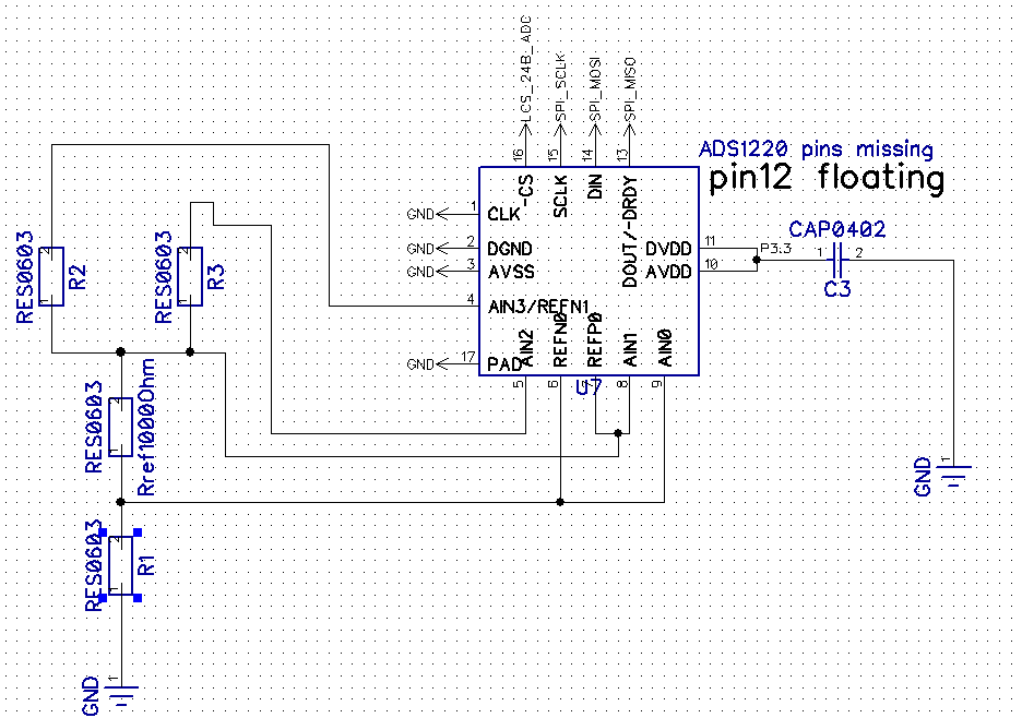
We use the DAC1 current (1.5mA) to create a voltage drop over two resistors that we want to measure and a reference resistor. The DAC1 current affects properties of our device, but that is not a problem if it is constant/stable. It is not.

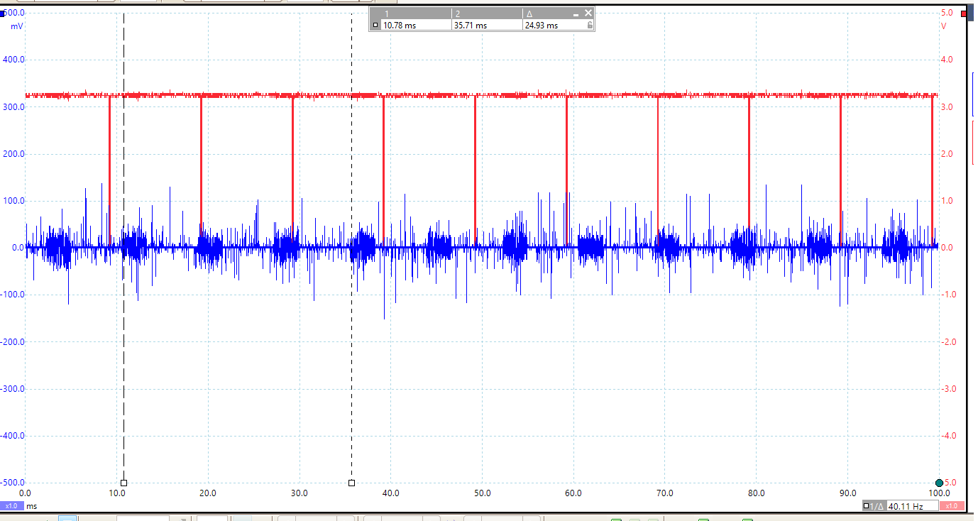
Our resistor chain is Input - R1 - REF - R2 - GND and Input - R3 - REF - R2 -GND. We are measuring R1, R2, R3 and internal thermistor. After 10ms we switch to the next measurement. One conversion takes about 6ms (so total cycle time is 40ms). In the first interval we input the DAC1 current in R1; for all other cycles we input in R3. Measurement is set to be continuous.

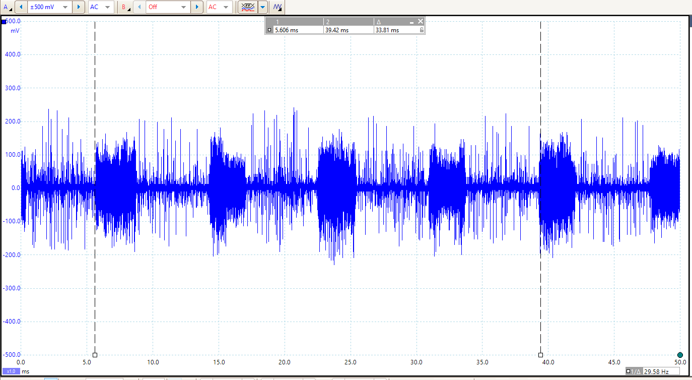
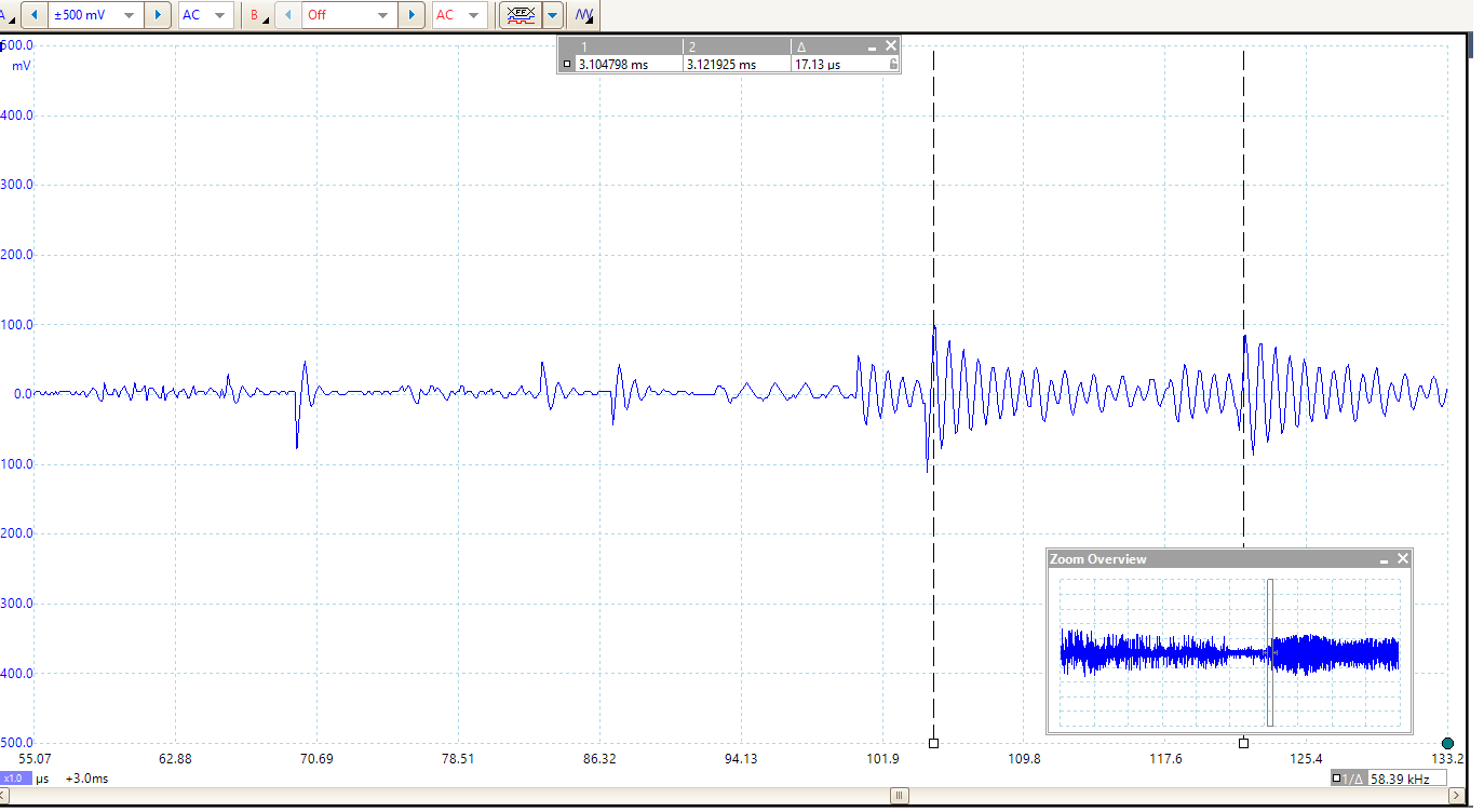
The expected behavior is that the current in the R2 resistor is constant (with 2 short periods of switching input from R1 to R3 and back). We see that it is not and after each conversion there is noise on the voltage over R2. The noise has a repetition rate of about 60kHz (looks like an excitation) and then a ringing at 1.2MHz. 

Why would the DAC1 current not be constant from conversion to conversion (as indicated, we set measurement to be continuous)? After the first conversion (6ms), the 2nd conversion will not be completed, but that should not impact the DAC1 current.

Any thoughts on why the DAC1 current would show an excitation/ringing behavior?

Thank you,

  • Hi Heino,

    There is a lot of missing details.  It would be very helpful to see an actual schematic of the ADS1220 connections supply configuration and resistance values being used.  It would also be very helpful to know the specific registers settings being used as well as how the inputs are connected.  It is not clear to me what you mean by internal thermistor?  Do you mean the internal temperature sensor of the ADS1220 or do you have some other thermistor in your circuit?

    In general, the IDACs are designed for ratiometric measurements.  In this way most noise and IDAC drift would cancel in the measurement.  Are you using the REF resistor in this way?  It is also important that the IDAC compliance be met.  The total voltage drop across all elements in the current path must be less than AVDD - 0.9V with respect to AVSS.  Not meeting the compliance voltage is the usual reason why the IDAC output is inconsistent.

    To be honest, I have never actually looked at the IDAC output in terms of noise.  The ADS1220 will cancel the high frequency noise unless the noise aliases back into the passband.  It is important to have some antialiasing filters on the measurement inputs.

    It is unclear as to how the current is being delivered or to the total current path.  One thing to consider is the input ranges of the measurements.  For example, when using a unipolar analog supply, measurements referred to GND must disable and bypass the PGA.  This reduces the input impedance and also may result in charge injection appearing on the inputs which may be part of what you are seeing.

    Best regards,

    Bob B

  • Thank you for the response Bob. 

    I have attached some clarification (hopefully). The circuit is attached, with the reference resistor in the middle and the R1 always in the circuit and R2/R3 in the circuit dependent on where we inject the DAC current. We do a ratiometric measurement with the reference resistor as the divider. Typical values for R2/R3 are 700 Ohm and R1 300 Ohm. I do see your point on the AVDD (3.3V) and we are likely not meeting the -0.9V buffer (with the resistance values we are probably at 3V). I can reduce the current to address that issue. We are disabling the PGA. However, we are not seeing any issue during the first convversion. 

    The register settings for the 4 measurements are:

    0x41 0x04 0x47 0x80

    0x31 0x04 0x47 0x60

    0x81 0x04 0x47 0x60

    0x01 0x02 0x47 0x60    (this is the internal temperature sensor)

    In general, I think that the actual measurement is not a problem (the values seem OK). Our issue is that the DAC current on R1 actually impacts the physical parameters of that device it is in. So our desired behavior is that the current is constant. Right now we are seeing that every 40ms (the above 4 cycles) we see an excursion in one of the performance metrics.

    The second graph shows the voltage at the reference resistor (between Rref and R1) during the full cycle. As you can see we have 4 cycles. It looks like that the signal gets much noisier after the first conversion, which surprises me, as we are doing continuous measurements. The third graph is a detail of the voltage at the transition between clean and noisy (which I believe is directly after the first conversion), with some excitation behaviour and ripple.

    I hope this clarifies my problem a bit. 

    Thank you,

    Heino

  • Hi Heino,

    There are a couple of things I noticed in the schematic.  If you are sourcing current through the mux and also measuring the input through the same pin, you will see an error as there will be a voltage drop across the mux input switch.  The value of the resistance can change over temperature, so in this case there could be a fluctuation of the measured voltage.

    Your 3rd measurement is showing AIN0 to AVSS (across R1).  This is outside of the input range with the PGA enabled.  So this value could also easily drift and will be non-linear.  If you are going to measure this resistance, then you are required to disable the PGA.

    The noise you are showing in your plots may be from the power source.  If you are using a switched mode power supply, I would check to see if there is similar behavior on the supply.  You may need to add some supply filtering and perhaps some larger value caps at the ADS1220 input supply pins.

    You may also benefit from adding differential caps across the measurement input pins.  I personally would change the circuit so that I would have proper antialiasing filters at the inputs.  This could be done by adding an external current mux (or switch) and an additional mux to switch the inputs.  This will of course add some analog settling time to the measurement, but will eliminate the error of the current flowing through the input being measured.

    Best regards,

    Bob B 

  • Thank you Bob,

    This is a preliminary response, just to let you know status. First of all, your comment on the PGA triggered me to take a closer look. I had intended to disable the PGA, but misread the register definition (1 for disabling, whereas I though 0 for disabling). So I will fix that and see if it resolves my problem.

    I don't fully understand your comment on the voltage drop over the input switch. I would expect the measurement point to be at the pin, so the input switch for the IDAC current would be before the measurement point. 

    I have my doubt that the noise is from the power supply, as the noise is not present during the first ADC conversion and afterwards it is there. So there is some change in the noise triggered by the ADC operation.

    A lot of the design choices are triggered by space limitations. The board is very small (driven by the product around it) and adding components is going to be painful. Though it may be worthwhile, so I will be looking into it. 

  • Hi Heino,

    The ADS1220 internal clock oscillator frequency is 1.024MHz in normal mode (2.048MHz turbo).  The actual over-sampling frequency is 256kHz (modulator frequency) and the input chopping frequency would be about 1/4 of that.  As the chopper will create an input bias current, this will couple with the IDAC current as you are using the same pin for both IDAC current and measurement.  

    Although this is technically possible, there is no way to prevent external noise from aliasing back into the ADC conversion.  As to the noise you are seeing, the noise shows in hundreds of mV in your scope shots.  This is not at all expected.  It is possible that large artifacts are showing up while operating outside of the IDAC compliance, but this is much greater than I would expect.  Do you see this noise on all of the measurements or just for R2?  Does the noise reduce when operating in the correct compliance range?

    Best regards,

    Bob B

  • Thanks Bob, 

    Thank you for confirming those frequencies. They kind of align with the frequencies I am seeing, suggesting that they are somehow seeping into the IDAC ouptut. 

    I also need to take my earlier comments back. I did actually bypass the PGA in all my testing, so that was not the issue.

    I was able to gather some additional information by capturing the SPI communication window (red trace, low when talking, gets the latest value and sets up the next measurement). It turns out that the noise is not linked to the conversion cycle. (I don't know where the 120Hz frequency of that signal would come from).

    I will be trying a couple of additional things: 1) try lower IDAC current to get the max voltage in compliance; 2) try single shot mode as I learned that the IDAC remains on between shots and 3) change the sequence of setting registers (first set IDAC current, then connect IDAC and then do the rest). I will see if these things have an impact.

    I will also add a cap over the R1 so that hopefully any remaining noise gets smoothed out.

    Thank you,

    Heino