This thread has been locked.

If you have a related question, please click the "Ask a related question" button in the top right corner. The newly created question will be automatically linked to this question.

DAC80004EVM: Connecting Jlink EDU to DAC80004EVB

Part Number: DAC80004EVM
Other Parts Discussed in Thread: DAC80004

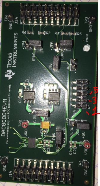
Hello, I have bought DAC80004EVM shown bellow.

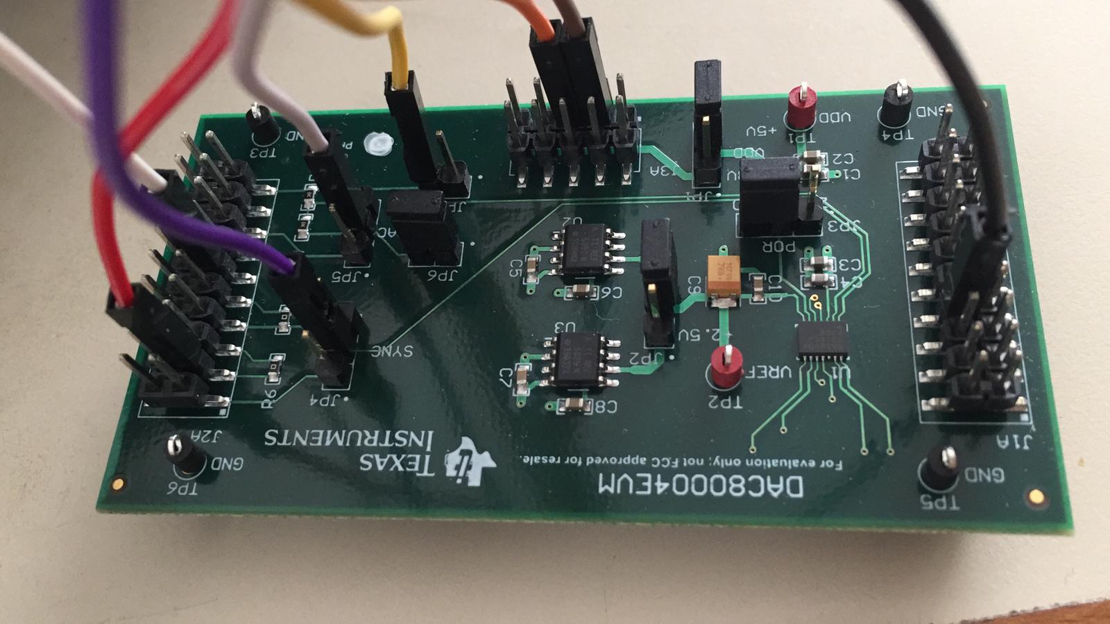
I want to program it  using Jlink debugger with pin out shown bellow in the poto bellow on the left.
Where do connect the Jlink pins on the DAC80004 board?
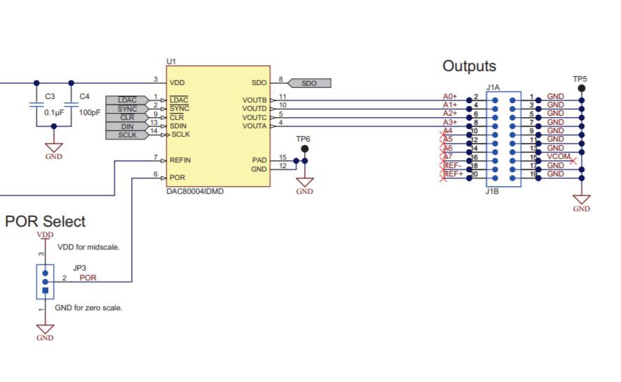
Also regarding the Vtref pin,i need add a voltage source to the board an connect Vtref to it?

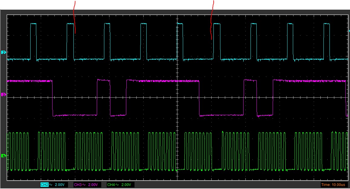
I have programmed DAC80004 before ,the chip was on board ,I connected to the board using JLINK SWD connection, and i communicated with the device using SPI commands.
I want to connect to DAC80004EVM with my JLINK EDU and communicate with it using SPI
Thanks.

  • Yefj,

    I'm not too familiar with the J-Link connector pinout and functions, so I may not be able to answer all of your questions about it. I'm not even sure you can use the JTAG debugger to emulate SPI. I had to look online for some more information. Where did you get the picture for J10? It's not on the schematic for the DAC80004EVM. The EVM schematic only has header pins for J1A, J2A, and J3A.

    Digital connections for the EVM come in primarily to J2A (on the right side of the board) shown below:

    Of these connections, the SYNC, SCLK, and DIN are the most important.

    Based on what I've read, pins 14 16 18 and 20 might be used for other firmware purposes, so I would select a different ground pin. Based on the description VTref, you would connect this to the VDD of the target device. It sets the output logic levels. I think TDI is the data input for SDIN and TCK is the data clock which would be SCLK. TMS is the JTAG test mode select, but I don't think it's used as the data input. Again, I'm not too familar with the JTAG standard.

    I did note that some JTAG devices can emulate SPI. I did find one manual that had this pinout for SPI:

    You should check to see if your JTAG debugger has this option to emulate SPI.

    Joseph Wu

  • Hello Wu,Ok i understand that we can work without the JLINK debugger.So by connecting diectly DIN,SDO,SCLK,SYNC,LDAC,CLEAR from my controller.

    Where do i connect the VDD on The DAC80004EVB BOARD,What kind of VDD value to USE?

  • Yefj,

    You should read through the DAC80004EVM User's Guide. You can find the link here:

    https://www.ti.com.cn/cn/lit/ug/slau689/slau689.pdf

    In the user's guide, you can find more about descriptions for the pin headers and other features of the EVM. At the end of the pdf, there's a schematic for the board, and it looks like you have options to connect the VDD to 5V or 3.3V. You could start with the connection at J3A and use the jumper at JP1. I pulled a snippet of the schematic for you below:

    Joseph Wu

  • Hello Joseph,I want to use 5 volt VDD .So I put the plastic thing as shown in the red marked circle.

    In J3 i marked the pins as 1,3,5 on the photo in the middle so i need to put at pin3 5V at pind 5 GND? 

    Correct?

    Thanks.

  • Yefj,

    Again, I would look back at the schematic for the EVM in the DAC80004EVM user's guide. You can find the complete schematic to the board in the pdf.

    Going back to the the snippet, you would connect +5V to pin 3 of J3A and the ground to pins 5 or 6 of J3A.

    If you have clip leads, it may be more convenient to connect the +5V to TP1 and the ground through TP4.

    This second method may be a bit easier. TP1 and TP4 are also both shown on the snippet of the schematic, and in the user's guide, you can see that the GND and VDD go directly to the device.


    Joseph Wu 

  • Hello, I have connected on J3A pin3 5V pin5 GND.
    So U1 VDD will have 5 volts.
    I want to connect Ldac=0 CLEAR*=Vdd  POR=0 REFIN-5V (if thats correct for DAC)

    Sync is the chip Select and its controlled JP4 and set as shown in the board photo

    So is for LDAC i want it to be 0 and its controlled with JP5

    How do i connect to the SYNC Input signal on the board?

    How do i see that LDAC is zero with this setting?

    Thanks.


    https://www.ti.com.cn/cn/lit/ug/slau689/slau689.pdf?_ticdt=MTYxMDEwNzkzOHxsaXQ5YmYxMDQyMDliZjEwNDIwOWJmMTA0MjA1ZjI5MDY0NTI5MjRmOTAxfEdBMS4yLjE5ODYyMDgzMDIuMTU5NjUzODMwMHwx

  • Yefj,


    For the DAC80004, the /LDAC signal is used to load the DAC value into the register to set the output of the DAC. This is a digital trigger that idles high and then transitions low to set the value (and then returns high, ready for the next DAC write event).

    /CLR is a DAC value register clear. If you don't intend to clear the value (or write to it to set every value) you can set it permanently high. The POR value sets the initial value of the DAC at power up. With POR=0V, the DACs all power up to 0000h for a DAC value.

    REFIN is the reference voltage. With VDD=5V, the REFIN can be set to 5V as well. Note that if you used a smaller VDD value (between 2.7V and 4.5V), the REFIN can only be as high as VDD-0.2V, based on the Recommended Operating Conditions shown in the datasheet.

    You can connect digital signals through the existing jumpers on the board.

    /SYNC - pull out the jumper on JP4 and use the middle connection
    /LDAC - pull out the jumper on JP5 and use the middle connection
    /CLR - use the right side connection to JP7

    When you have these connections set up, I highly recommend using an oscilloscope or logic analyzer to see the digital signals to know that the device is being controlled correctly.

    Joseph Wu

  • Hello Joseph, LDAC=0 CLR=1 (3.3V)

    I want to use "Write to buffer n and update all" command to present analog value to channel 0.
    {00000011,b00001111,11111111,11110000}; channel 0(register 0) write FFFF expect to get full scale VDD
    so in hex the command is 0x03,0x0F,0xFF,0xF0
    So if so far everything is correct the SYNC(purple) LDAC (GRAY) CLR*(Yellow) wires are connected as you shown in the photo bellow.
    So for my write and update command to work properly i need to connect gray to ground and Yellow to 3.3V.

    Then in the later photo shown bellow i connect J3A pin3(Brown) 5V and Pin5 (Orange) GND.

    On the final spet i go to J2A pin3 and connect red wire to it, this is CLK.
    Then J1A pin8 is Black wire is output of channel 0.

    Then J2A pin 11 connected to white  wire which is SDIN(MOSI) port.
    POR i didnt touch i leaved it as it is. and the full wire connection in as shown in the last  photo.

    In the last SPI photo i show the SPI signal on the scope

    and instead of VDD i get NOTHING on channel 0
    Where did i go wrong?
    Thanks.


  • Yefj,


    I haven't reviewed all of your post and connections to the EVM. However, there are two problems with your communication that I noticed very quickly.

    First, assuming that the blue trace in your oscilloscope is the /SYN, you have the /SYNC pulse rising between each byte in transmission. If you look at the stand alone timing in the datasheet, you can see that the /SYNC stays low between all the bytes of the communication. /SYNC should stay low for a total of the four bytes (32 bits). You can see this below:

    Second, the supply of the DAC80004 is set to 5V, but the digital communication is set to 3.3V. Voltages that determine the digital high and low are typically based on the supply voltage. For the DAC80004, this is not a problem with the digital inputs, and because the digital input highs and lows are within the 0 to 3.3V range. However if you are using the digital output, the SDO line may be trying to drive out a 5V signal which might be a problem for whatever microcontroller you use. I would either disconnect the SDO if you're not using it or use some series resistance to reduce any current that might be going to the microcontroller.

    Joseph Wu

  • Hello,Is there a test point for the SYNC SCL SDIN LDAC etc.. so i can see exactly what went into the DAC80004 device?

    Thanks.

  • Yefj,


    You can just check the EVM user's guide to see all the connections to the device on the EVM. Again, I'll place an image of the digital connections here:

    There aren't many extra connections to connect the digital lines to the board and to connect a test line. As you can see in the figure, the CLR line has a connection to pin 2 of JP7 and to pin 19 of J2A. The /LDAC line has a connection to pin 2 of JP5 and pin 2 of JP6.

    After that, if R6 has a resistor populated, then you can connect to pins 3 and 5 of J2A to get to SCLK, If R7 is populated, then pins 7 and 9 of J2A can be used to get to /SYNC with the jumper on pins 2 and 3 on JP4. Unfortunately, there aren't any extra leads for DIN and SDO.

    However, on the bottom of the board there may be unpopulated J2B that connects to the pins above. If you were to solder another connection to those pads, you could attach test wires there.


    Joseph Wu

  • Hello Joseph , I am sending SPI DATA  commands in 3.3V ,I set the VDD to be 3.3V by pinning JP1  VDD to 3.3V side and putting J3A pin9 to be 3.3V.

    And  by using {0x03,0x0F,0xFF,0xF0} command i get 3.3V on channel A
    Is there a way i could get channel A output voltage maximum  as  5V?
    Thanks.

  • Yefj,


    The output of the DAC is limited by the supply voltage. If the VDD and reference is set to 3.3V, then the maximum output is basically limited to 3.3V. This is listed in the output characteristics section of the electrical characteristics table in the datasheet:

    Because the output is buffered, the output won't quite reach VDD or GND because of the drive limitations of the op-amp. This is described by the headroom characteristics also listed.


    Joseph Wu