This thread has been locked.

If you have a related question, please click the "Ask a related question" button in the top right corner. The newly created question will be automatically linked to this question.

ADC12DJ5200RF: ADC Multi Chip Synchronization

Part Number: ADC12DJ5200RF
Other Parts Discussed in Thread: LMK04828

Hi,

We need to Synchronize two ADC12DJ5200. The sampling clock of both the devices is being generated by a single PLL and both the clock trace lengths are matched on board. We are using the device LMK04828 to generate the device and SYSREF clocks required for JESD204B. The SYSREF trace lengths from LMK to ADC are also matched. The Device clock and SYREF pairs to the FPGA are also length matched. We are operating the ADC in JMODE 20 with a sampling rate of 5.2Gsps 

With this, the phase of the data captured between the two ADCs is varying at every power cycle. Please clarify at  what stage of the Initialization Setup(Section 8.3) should The Automatic SYSREF Calibration mentioned in Section 7.3.6.3.2  of the datasheet be done.

Regards,

Ayesha

  • Hi Ayesha,

    Please send me a block diagram of the system setup for the 5200RF synchronization.

    I will work on verifying the initialization setup in the meantime.

    Regards,

    Rob

  • Hi Ayesha,

    I was thinking about this more, can you please check the time alignment of the sampling clock and sysref clocks at the two ADCs, as close as possible?

    Are those in phase after each power cycle?

    Getting us the block diagram and also the spi reg writes for both the 5200RF ADC and LMX04828 would be helpful as well.

    Regards,

    Rob

  • Hi Rob,

    Thank you for the response.

    Please find Attached the ADC clock tree and PLL and ADC register settings.

    We had checked the SYSREF timing between the two ADCs  which is constant at every power cycle. It is difficult to check the phase between the Sampling clock and SYSREF of the ADC as this is an FMC design and we do not have access to probe the sampling clock. However is it important that they remain in phase? As we assume that even if Sampling Clock and SYSREF are out of phase at every power cycle, the Automatic SYSREF Calibration feature of the ADC would align to the clock to SYSREF. Please confirm if our understanding is correct.  

    Also, we are not sure at what step should we perform Automatic SYSREF calibration.

    We also had an observation that for both the ADCs the SYNCSEn signal from the FPGA goes high at different time intervals in the JESD IP Core. But, in the current design, we are passing the signals through AND gate in the FPGA. The AND gate output is given to the two ADCs. 

    Regards,

    AyeshaClock_Design.7z

  • Hi Ayesha,

    I think I need a reconfirmation, sorry for the confusion if this wasn't written more clearly.

    Is the sample clock or both ADCs in phase and is the sysref clock of both ADCs in phase with each other? They need to be.

    Please probe at the nearest component...for the sample clock to check this.

    The sample clock and sysref clk do not need to be in phase with each other, which appears to be what you answered. Again, I apologize for the confusion.

    No need to use the auto sysref cal, Instead use the sysref windowing feature, this register is called SYSREF_SEL. Use this and program, a valid value for both ADCs and read the SYSREF_POS register, all 1's are not valid, 0's are valid, then pick a position and write that value into the SYSREF_SEL register to meet the setup and hold times.

    Also, can you clarify this statement a bit more from above?....With this, the phase of the data captured between the two ADCs is varying at every power cycle

    Does this mean the data is in phase between the two ADCs from data capture to data capture but when you power cycle either of the two ADCs they are now out of phase when capturing data?

    If there is still questions, please let me know and we can setup a call.

    Regards,

    Rob

  • Hi Rob,

    Yes, the sampling clocks and the SYSREF are mutually in phase at every power cycle.

    We had been working on this. There was an issue in the data capture within the FPGA that caused phase incoherence. The issue is now resolved. 

    Thanks for the help.

    Regards,

    Ayesha

  • Hi Rob,

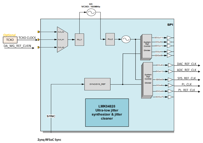
    We are developing Zynq RFSoC based board for 64CH ADC sampling. For the same, we are using 4 RFSoC boards each with LMK04828 CLK synthesizer.

    The CLKIN for all the LMKs is from single oscillator source.

    Since we need to sample all ADC channels with as less as possible phase delay, so could you let us know how to SYNC multiple LMK04828 ?

    If possible, please share your email id, so that we can discuss in details.

  • Taking this offline to discuss via email directly.

    Regards,

    Rob