This thread has been locked.

If you have a related question, please click the "Ask a related question" button in the top right corner. The newly created question will be automatically linked to this question.

ADS125H02: CRC-2 conversion for SPI command

Part Number: ADS125H02

Hi,

I am trying to communicate ADS125H02 with SPI protocol for device ID command i sent [ RREG 0x20 0x00 0xEB 0x00 0x00 0x00 ]  i got response as [0xFF 0xA0 0x00 0x6B 0xFF 0x80], i thought i got device ID , once I exceuted RREG [0x22 0x00 0xEB 0x00 0x00 0x00] i am getting the same output  [0xFF 0xA0 0x00 0x6B 0xFF 0x80], i tried to caluculate CRC in different and provided different values but unable to get correct data even for the DEvice ID , does the CRC has to be calculated for 40 bits, or only the the two command bytes.

Thanks & Regards

Sasikumar E

  • Hi Sasikumar,

    In most cases the CRC is a two-byte computation - as you can see from Table 24 in the ADS125H02 datasheet, Byte 3 for DIN is "CRC-2", which means is the CRC computation of the previous two bytes.

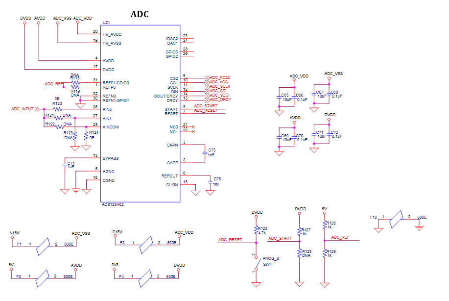
    Can you send me a schematic of your system so I can see how your device is configured? Also, can you take logic analyzer and/or oscilloscope shots of your digital communication lines? I would guess that something has gone wrong in the communication such that the ADC is not receiving your inputs correctly.

    -Bryan

  • Hi Bryan,

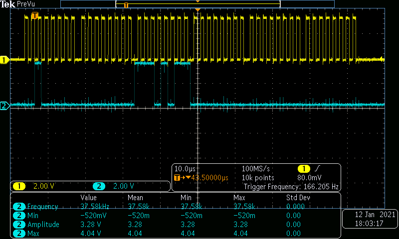
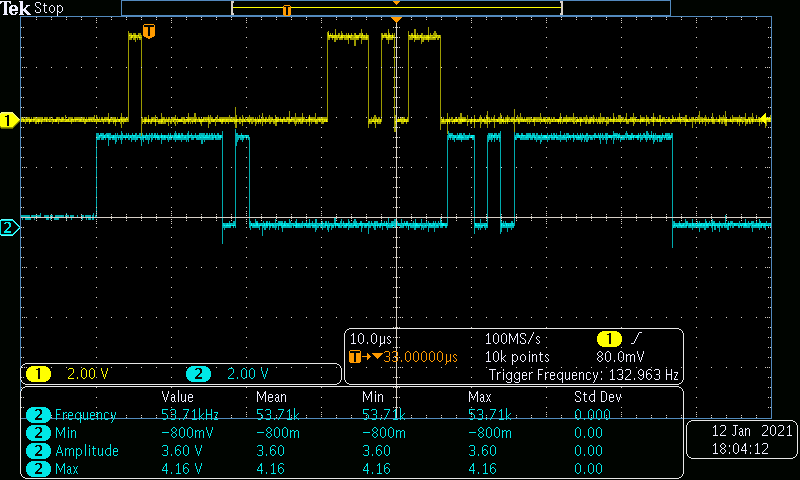
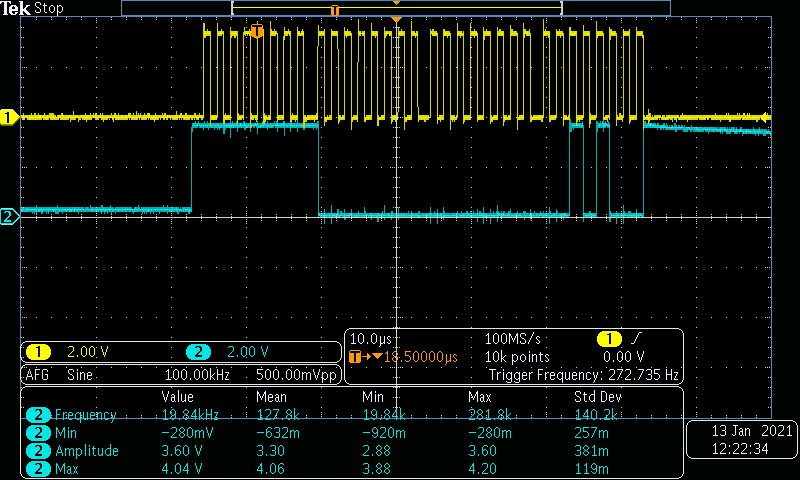
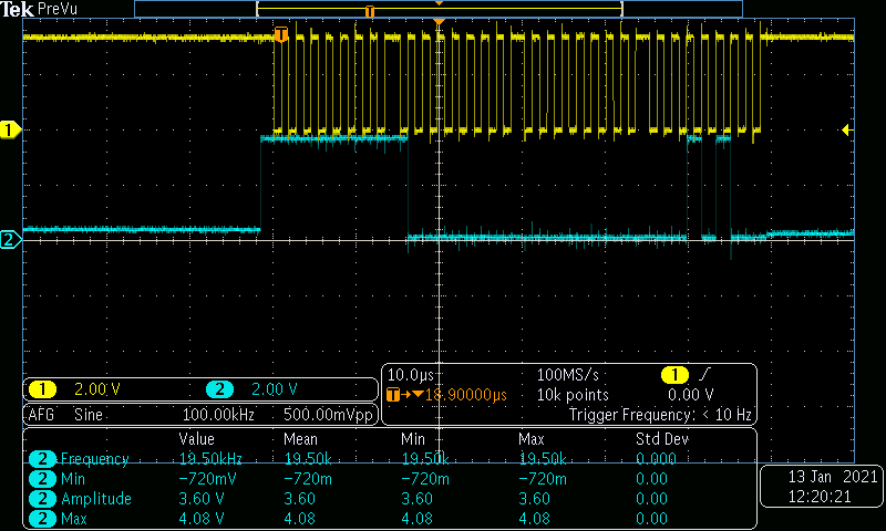
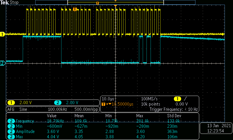
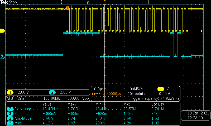
    Kindly find the attached images for schematic, chipselect , clock, data input, data output

  • Hi Sasi,

    If I look at the second scope shot that you sent, it appears that you are latching data on DIN on the rising edge of SCLK. Please note that the H02 requires data to be latched on the falling edge of SCLK, per section 9.5.1.3 on pg. 45. I believe correcting this should solve your issue. Please also make sure that DOUT is latched on the falling edge of SCLK.

    -Bryan

  • Hi Bryan,

    I think I have provided the DIN on the falling edge of the clock, do I want to change the polarity and then provide the falling edge of the clock, yet I am trying all the four MODE of SPI, initially I tried for the NOP command as DIN [0x00, 0x00, 0x00, 0x00] and DOUT mode0 is [0xFF,0X80,0X00,0X14], MODE1 [0XFF,0X80,0X00,0X14], MODE2 [0XFF,0X00,0X00,0X28], MODE3[0XFF,0X80,0X00,0X14] if MODE2 provides the correct output then how CRC-2 [0x00] gets related to OUT CRC-2[0x28] 

  • Hi Sasi,

    I am sorry, I'm not sure what your question here is? You cannot read back registers using the NOP command, so I am not clear how you are relating NOP on DIN to MODE2 on DOUT?

    Also, please note that the CRC calculation on the NOP command (CRC of [0x00 0x00]) is not 0x00 as you have shown, but 0xD7. So the correct NOP command should be [0x00, 0x00, 0xD7, 0x00], assuming that Byte 2 = 0x00.

    If the CRC you send on DIN does not match the ADC's calculation, the ADC responds with the inverted CRC value to let you know that something has gone wrong with the communication. Note that the inverted value of 0xD7 is 0x28.

    Please make sure you are sending the correct CRC value to the ADC with each DIN transaction. You can use our helpful calculator tool to understand how to perform the CRC calculations: https://www.ti.com/lit/zip/sbac234

    -Bryan

  • Hi Bryan,

    Thanks for the reply, our issue was the CRC-2 calculation, During calculation, we set the shift register initialisation value as 0x00;