This thread has been locked.

If you have a related question, please click the "Ask a related question" button in the top right corner. The newly created question will be automatically linked to this question.

ADS1299: Problem with test signal of ADS1299

Part Number: ADS1299

Dear colleagues

I have a problem with ADS1299.

I've implemented a portable 20-channel EEG device with three ADS1299 and STM32F407 microcontroller (MCU).

During operation test with a test-signal mode, we found that several channels were severely distorted due to unknown reasons.

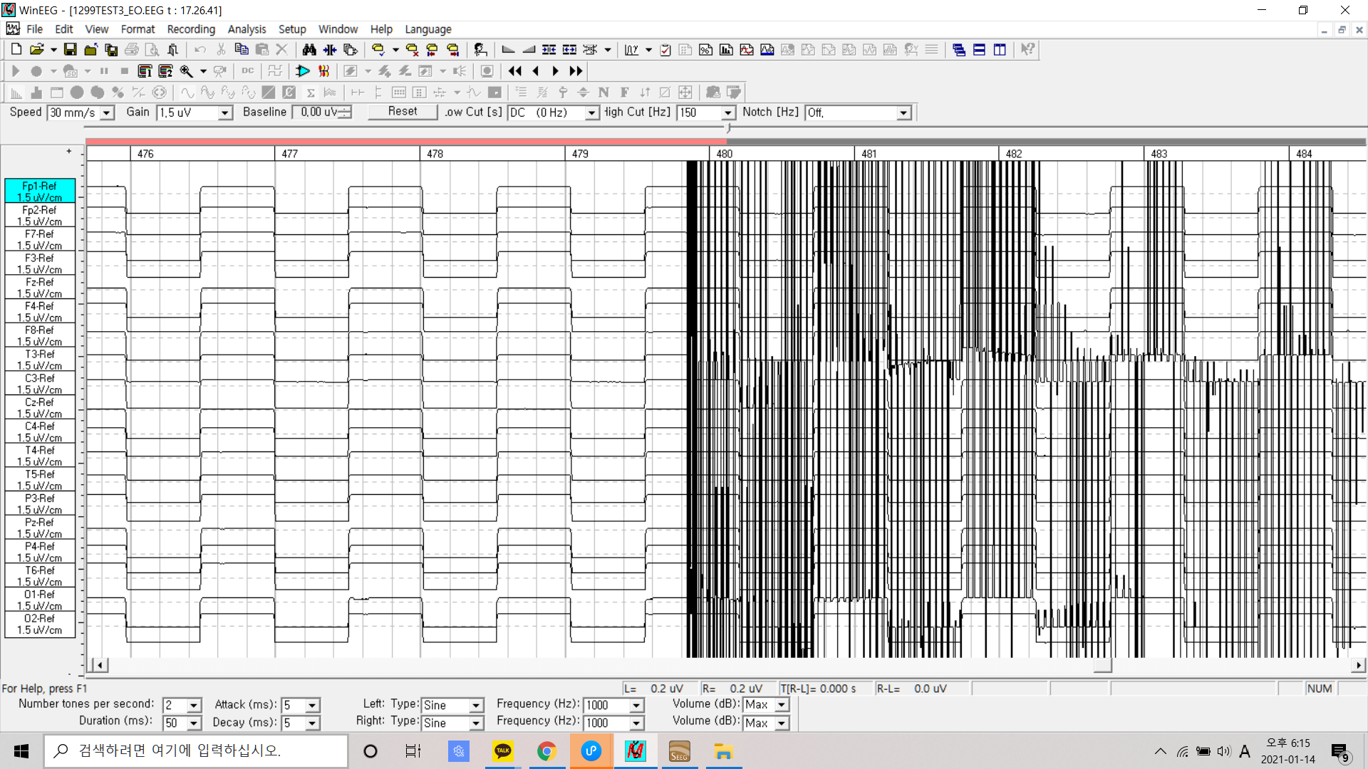
Please see the attached picture.

At first, the square waves from each channel were normal, but several channels were distorted.

(Test signals are overlapped, but several signals are normal)

The software engineer said that he inspected the data during SPI communication between the ADS1299 and MCU using STM Studio.

He said that the original test signals were distorted in ADS1299 and they were transmitted to the MCU.

My questions are....

1) Is it possible that the square test signals can be distorted due to several reasons, for example, an electronic circuit or test conditions?

2) If then, how can we fix this problem?


I will wait your useful advice

Thank you in advance

Best regards

Heejin Kim

  • Hi Heejin,

    Welcome to the E2E forum and thanks for your post. 

    The internally-generated test signal is derived from the VREF signals and any distortions or glitches on the VREF signals can couple into the system. Your plot shows the distortion starts after marker 480 and looks fine before that. Is there any external circuitry on the hardware that was enabled during this period? During this time period, the VREF signals may be corrupted and cause glitches to appear on the output.

    Can you perform the same exact test with the input shorted?

    Thanks.

    -TC

  • Dear TC

    Thank you for your reply.

    I asked our development team to check whether the VREF was also distorted while the internally-generated test signal was distorted. 

    However, the VREF voltage was constant (appeared on the oscilloscope screen).

    Then, is there another possible cause for this problem?

    Thanks

    Heejin Kim

  • Hi Heejin,

    The distortions can also couple from multiples places such as the power supply, ground connection, analog references, and digital circuitry. Does this happen only to the test signal mode only or also appears with different input? It may be useful to check to see if you see the same issue with the input shorted test and other DC test mode signal.

    Thanks.

    -TC 

  • Thank you for the advice!

    Actually, we did not perform the test with the input shorted, but, the same result appeared with the normal input condition. 

    Thanks

    Heejin Kim

  • Hi TC,

    i have some questions for actual tests.

    1. in fact we already tested with MUXn[2:0] register to 101, to make 1Hz square test signal.

    but if we want to test input shorted as you said, we cannot test with 1Hz signal. is it okay?

    What should we check with input shorted signal?

    and what does it mean "other DC test mode signal"? can you guide for this test?

    2. is there any possibility that SPI communication goes wrong and make some noise?

    3. in first PCB we did not design analog ground and digital ground separated. can it be make some problems related to noise?

    Please Check these issues. Thanks.

    Best regards,

    Chase

  • Hi Chase,

    Please see my comments inline below.

    1. in fact we already tested with MUXn[2:0] register to 101, to make 1Hz square test signal.

    but if we want to test input shorted as you said, we cannot test with 1Hz signal. is it okay?

    >> Yes, it is fine to switch from 1Hz test signal to the input shorted test by changing the MUXn[2:0].

    What should we check with input shorted signal?

    and what does it mean "other DC test mode signal"? can you guide for this test?

    >> By changing the MUXn[2:0] from 101 to 001, the analog channel input will now be shorted internally to (VREFP+VREFN)/2. You should be able to see the noise performance of the device in this test mode. Please refer to Table 1 to Table  4 (page 16-17) for the expected noise performance with different test conditions. By "other DC test mode signal", I meant you could also check for MUXn[011], which will give you the supply measurements (Please see Section 9.3.1.1.4). You can also set a know DC input externally with a DC signal source.

    2. is there any possibility that SPI communication goes wrong and make some noise?

    >> It is possible that the SPI communication goes wrong and causes the data to be incorrect. You can verify the SPI data communication by verifying the content of the 24-bit status bit on the data output. You should always get 0b1100 +  LOFF_STATP + LOFF_STATN +bit[4:7] of the GPIO register. Please refer to section 9.4.4.2 and section 9.5.2.4 for more information on the data output format. 

    3. in first PCB we did not design analog ground and digital ground separated. can it be make some problems related to noise?

    >> It is possible to have noise coupling from either the analog or digital ground planes. There is some layout recommendation for the device in Section 12 of the datasheet.  

    Thanks.

    -TC