This thread has been locked.

If you have a related question, please click the "Ask a related question" button in the top right corner. The newly created question will be automatically linked to this question.

ADS125H02: Unable to read correct data

Hi Bryan,

Initially, we want to configure it for single-channel single-ended negative voltage ADC conversion, we selected the internal reference of 2.5v

and finally started a conversion, when read through the RDATA register we are not getting the desired output, it generated a random digital value when cross verified for the analog value, we found that AINCOM produces 2.8v and AIN1 produces 10.7v varyingly. Is there a possible way to program this IC for single-ended conversion?

(first byte, second byte, CRC-2)

Reference Configuration (REF) Register    (0x46,0x10,0x82)

MODE4         (0x50,0x23,0x32)

START             (0x08,0x00,0x7F)

  • Hi Sasi,

    The H02 will always measure between two of the three input channels. This is indicated in the MODE4 register. So if you want a true single-ended measurement, you would need to connect one of these inputs to GND (most likely AINCOM)

    In the schematic you sent in your previous thread (https://e2e.ti.com/support/data-converters/f/73/t/969882) you have AINCOM tied to ground through a 0ohm resistor, so this should be okay.

    What is the voltage you have applied to AIN1? If you are leaving your inputs floating, they could be anywhere within the supply range.

    -Bryan

  • Customer response:

    Hi Bryan,

    AINCOM is connected to ground, AIN1 is connected to a pot varying from 0 to 3.3v, however, we did not get the desired digital value, so while checking the PIN the multimeter reads voltage readings from(2.8v to 10v) in AIN1 pin, and even at such high voltage levels the digital values are low and constantly changing from (0x00,0x00,0x02, to 0xDb,0xD1, 0x00) whereas most of the time I get the value of (0x00,0x00,0x02)

  • In reply to sasi kumar1:

    Hi Sasi,

    Can you apply a known voltage directly to the ADC inputs from a precision source and try to measure that back using the internal reference? That eliminates any issues with the pot.

    Just apply 1V between AIN1 and AINCOM, and make sure that AINCOM is grounded. Please send me the raw code results of these measurements as well as the oscilloscope shots.

    Also, you should be able to probe the DRDY pin on the H02 to see pulses at ~1/data rate in continuous conversion mode. This is another indication that the device is set to output data correctly. If you do not see these pulses in continuous conversion mode, the H02 is not outputting data.

    -Bryan

  • Hi Bryan,

    I applied precisely 1v to AIN1 and connected AINCOM to ground

    I provided three reference selections 

    1)internal reference selected(0x46,0x10,0x82)  and the RDATA value is(0x00,0x00,0x20)

    2) External reference (0x46,0x0A,0xC4) and the RDATA value is(0x00,0x00,0x20) REFN0 - 0V, REFP0-5V

    3) AVDD (default) and AGND (default) set as a reference this provides different values for  RDATA

    yet as you suggested i took the snapshot of DRDY with respect to MISO pin so even if the DRDY is high i am receiving

    yellow line - MISO output

    blue line - DRDY line

      data

  • Hi,

    i have not got any response kindly reply me

  • Hi Sasi,

    If you issue the RDATA command, the output should be 8 or 9 bytes long. In your last post you have only provided 3 bytes of data - can you provide the whole string of data when you issue the RDATA command?

    You also mentioned that the data varies for the case where VREF = AVDD/AVSS, but did not provide these values. Is the output data close to the correct value?

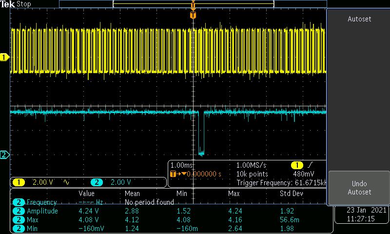
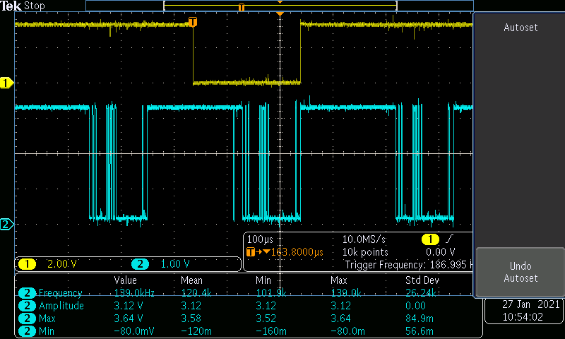
    I don't see DRDY pulsing in the images you sent. I only see DRDY transition (high, low, high) one time in the second image. Are you operating in continuous conversion mode or pulse convert mode? Can you put the device in continuous conversion mode, begin conversions, and then see if you can see DRDY pulses at 1/data rate? You do not need to read data during this test, you are just trying to see if the device is continuously updating DRDY.

    -Bryan

  • Hi Bryan,

    For the reference voltage, I am only using internal reference +2.5V & -2.5V. Since I am not getting the output i m trying all other combinations, 

    My DRDY pin is not getting low at all yet I am able to read values in DOUT pin yet not the correct value

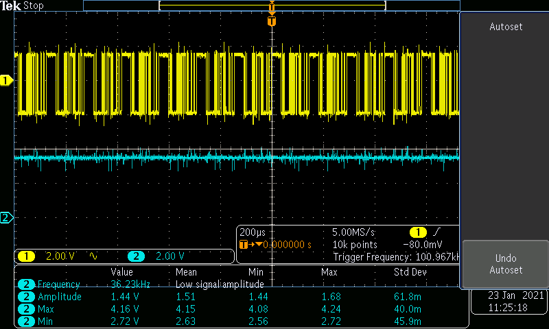
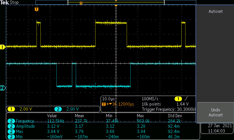
    First image RDATA output; yellow line - output, BLue line - clock;

    second Image yellow line -output, BLUE line DRDY

  • Hi Sasi,

    The data read transaction in the first image actually looks correct: 0xFF 12 00 AA 00 00 00 2B, where 0xAA is equal to CRC-2 of 0x12 00, and 2B is equal to CRC-3 of 0x00 00 00. This implies that you are not reading the STATUS byte, is that correct?

    • Are you sending the START command or holding the START pin high in order to begin conversions? If you use the START command
    • Are you using pulse convert or continuous conversion mode?
    • And what data rate are you using for these measurements?

    Again, I would try inputting a 1V signal directly into the ADC, use the internal VREF, put the device in continuous conversion mode, issue the START command, and see if there is activity on DRDY. Depending on the data rate you select you might have to zoom out on the oscilloscope's time scale in order to see multiple pulses.

    Also, please send a screenshot of DIN and DOUT when you issue the START command so we can see if the ADC is interpreting this command correctly

    -Bryan

  • Hi Bryan,

    I am using continuous conversion mode.

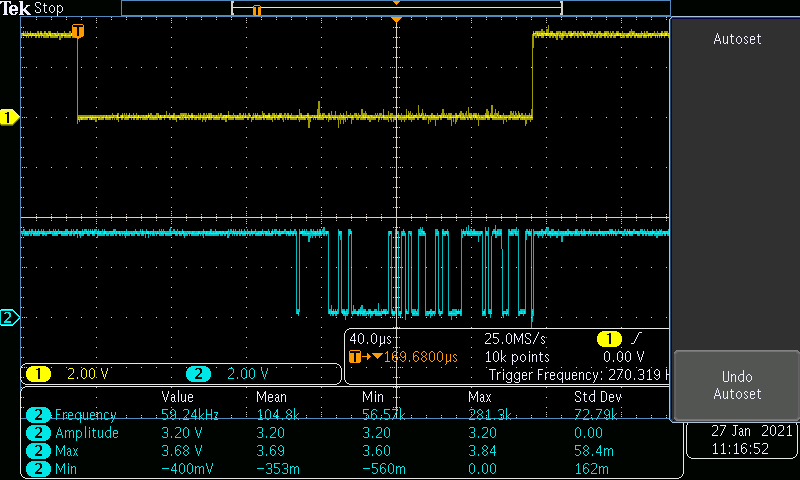
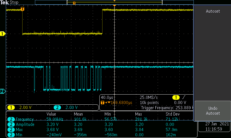
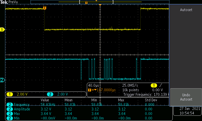
    IF I use START PIN to start my conversion random values are produced, the Yellow line is DRDY, and the BLUE line is DOUT, here the time duration also varies for outputs, since the time stamp provided is 40us for both.

    Now I am using the start command for starting the conversion, START pin is grounded,

    First image yellow line -cs, blue line clock

    Second Image blue line - clock,  yellow line DI

    third image - yellow line - DI, blue line - Dout

    without providing start command or 3.3V to the start PIN when I read the RDATA register I am getting the same output,

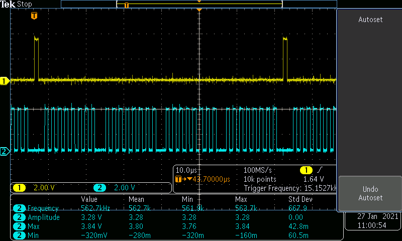
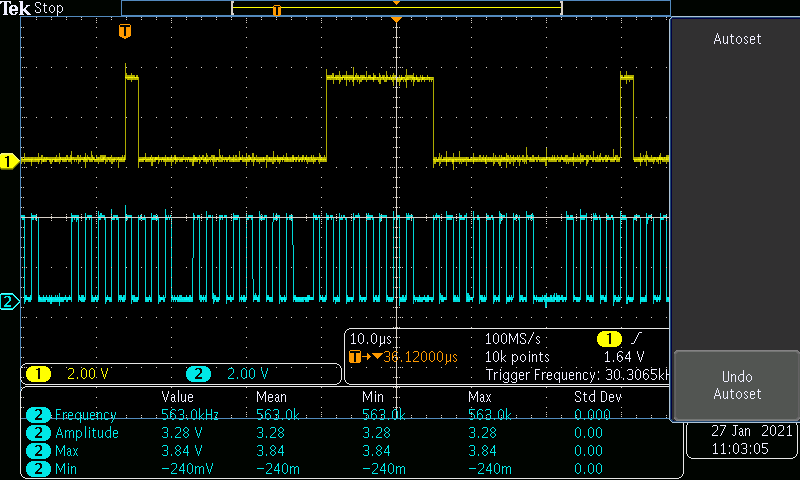
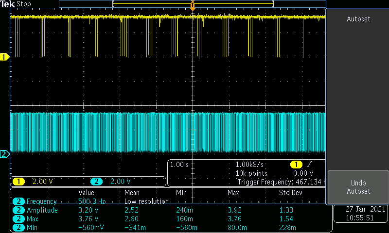
    I have set the default data rate of 20SPS, I have attached the images for 1s response where my DRDY line gets low more than 20 times , and even if the DRDY is high the DOUT provides the same output

  • Hi Sasi,

    Do you have a logic analyzer? It would make this much easier if I could see CS, DRDY, DIN, and DOUT all at the same time.

    I am not really sure what the signals are in the last three images you sent either, since they are not labeled. Is that DRDY and DOUT? If so, the second image shows DRDY going low multiple times in a row. To operate the ADC effectively, you should send the RDATA command as soon as DRDY goes low in order to make sure that you clock out data fast enough. Multiple pulses in a row suggest that you missed a conversion. Are you using the dedicated DRDY pin to identify when new data is ready?

    You can also try to read back the supply voltage and temp sensor using the MODE4 register (MUX[2:0] = 100b or 110b). If you are able to read correct data from the internal monitors, then something else must be incorrect at the input of the ADC.

    -Bryan

  • Hi Bryan,

    I don't have a logic analyzer,

    as you said they are DRDY and DOUT,

    as for the  second image I have set the default data rate of 20SPS, I have attached the images for 1s response where my DRDY line gets low more than 20 times, and even if the DRDY is high the DOUT provides the same output 

    In the MODE4 register I provided  (MUX[2:0] = 100b or 110b) and while reading RDATA i got (0x00,0x00,0x20) for both the commands,

  • Hi Sasi,

    Can you confirm that you are holding CS1 low and not CS2 during the START and RDATA commands? I know there were previous issues getting the CSx lines to operate properly.

    Also, have you enabled the STATUS byte as part of the data transaction? In one of the previous images you had sent 72 SCLKs to the device during a data read (9 bytes), but I didn't see a STATUS byte in the output. So this means that you are issuing 8x more SCLKs than necessary, which could cause some issues.

    I also noticed in your schematic that you have split ground planes (AGND and DGND) which we do not recommend. Moreover, I would increase the size of the cap on REFOUT to the datasheet's recommended value. I don't think either of these things are causing the issues at hand, but they should be considered for future PCB revisions.

    -Bryan

  • Hi Bryan,

    Sorry for the late delay  i was not able to work on the project.

    As per your suggestion I have checked CS1 and CS2 both are responding correctly when i am trying to program PGA cs1 is high and CS2 is low and vice versa when programming ADC.

    I have not enabled status byte so i reduced the clock cycles to 64 clocks yet I am receiving only 0x00,0x00,0x00 as RDATA value for temperature, HV supply Readback, and AIN1 

    i cannot figure it out what is my issue, My DRDY pin gets low but the data i read is 0x00,0x00,0x00 only yet when i check it with CRO i get various data

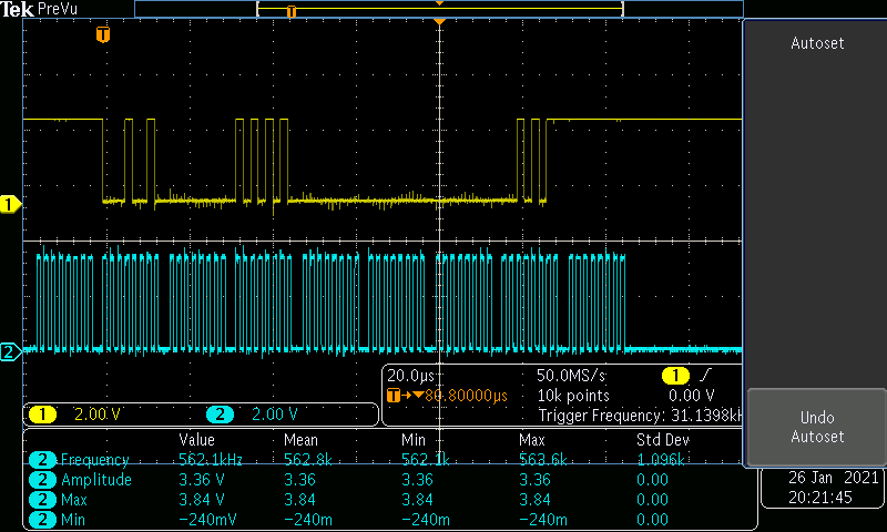
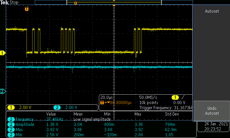
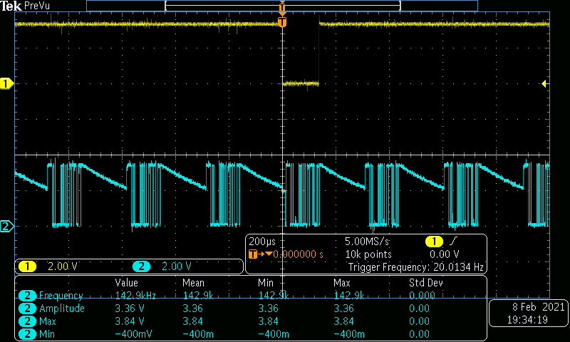
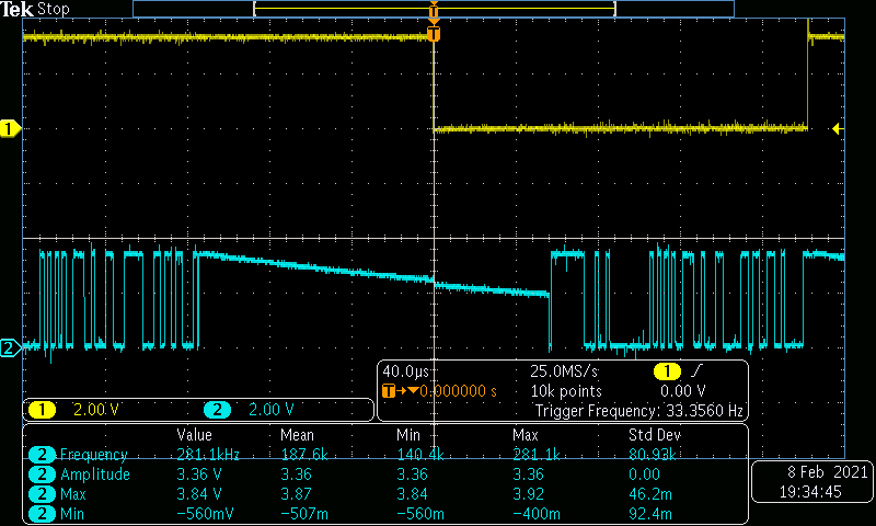
    yellow line - DRDY, Blue Line -MISO   

    DRDY gets only only when i start conversion by providing VCC in start PIN, when I provide GND to start pin and execute start command my DRDY pin does not go low, yet MISO pin receive some data

    Thanks & Regards,

    Sasikumar E

  • Hi Sasi,

    Why is there output on DOUT all the time, even when DRDY is high? Are you requesting data all the time? Is there activity on DIN at this point?

    If you are not sending commands to the device then something is wrong with the communication here, as you should only see data on DOUT once per data read. Please help me understand what is happening here.

    I will reiterate that this is where a logic analyzer would be very useful, so you can see all of the communication signals at the same time.

    -Bryan