This thread has been locked.

If you have a related question, please click the "Ask a related question" button in the top right corner. The newly created question will be automatically linked to this question.

DAC8562: Please review the schematic, and have some questions

Part Number: DAC8562
Other Parts Discussed in Thread: OPA2333

Hello TI experts,

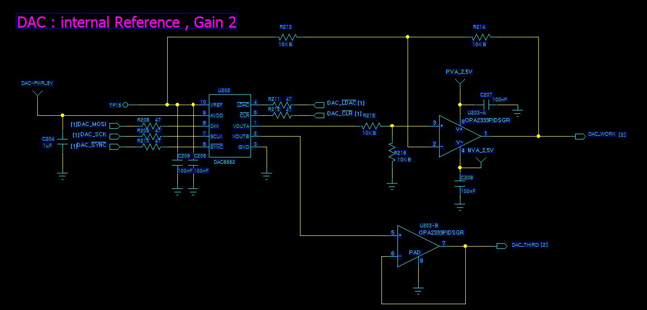
my customer designed schematic with DAC8562, please review the schematic below;

1. they want to use the output +/-2.5V for DAC_A. and DVCC/AVDD is 3.3V, use internal reference 2.5V, internal gain 2(default).

is it okay fir +/-2.5V bipolar output for DAC-A? or should we change AVDD to 5V or something? should we change any other else?

2. is there any way for increasing accuracy? my customer wants +/-0.1% accuracy. first of all DAC8562 can support this accuracy, and secondary i want to know something add to schematic for accuracy.

please check these issues. Thanks.

Best regards,

Chase

  • Hi,

    With internal reference of 2.5V and default gain of 2, DAC8562 max output will be 5V as per the transfer function.

    In this case with supply of 3.3V, you cannot use the entire DAC code range, it will saturate the DAC outputs. If you set the internal gain as 1 after the power up,

    DAC8562 will be at 2.5V max and depends on the resistor values in the op amp circuit you can achieve +/-2.5V. 

    Also I can see OPA2333 used in the output stage with +/-2.5V supply, there will be headroom issues with +/-2.5V. Look at the AOL specifications of OPA2333 its specified with +/-100mV from either supplies. if the op amp is not loaded, your best case will be +/-50mV from supplies ( at room temperature).

    For better accuracy, please have all the resistors at 0.1% or better in the output stage.

    Hope this clarifies your queries.

    Regards,

    AK

  • Hi AK,

    Thank you for your reply.

    actually my customer thought that they need +/-2.5V bipolar output, it is equal as +5.0V unipolar output. so the gain should be 2, and internal reference +2.5V.

    but as your saying, gain 1 and internal reference +2.5V is enough for +/-2.5V bipolar output. (under 3.3V AVDD) right?

    and how about R71 and R72? is it okay to remain these 2 resistors for +/-2.5V bipolar output? or should we remove/change the value?

    and could you explain more about headroom issue? I cannot understand it clearly.

    Thank you in advance.

    Best regards,

    Chase

  • Hi,

    Customer thought process is correct, but with 5V output, DAC8562 needs AVDD as 5V, not 3.3V.

    if AVDD is 5V, with internal reference of 2.5V and gain of 2, DAC8562's full-scale will be 0 to 5V which can be converted to +/-2.5V by the op amp circuit which customer has now.

    With 3.3V supply you can have +/-2.5V output by having gain at 1 and remove the 10K resistor which is connected to ground R72.

    OPA2333 output cannot swing to either supplies fully, with +/-2.5V, your output will be maximum +/-2.470 ( typical) and +/-2.450 ( worst case) at room temperature.

    OPA2333 has rail to rail inputs, but not true rail to rail outputs. Please see the output specifications below.

    Regards,

    AK

  • Hi AK,

    i checked schematic and your advice with my customer.

    customer said that they could not get +/-2.5V output if AVDD is 3.3V and gain is 1, then VOUTA will be 2.5V.

    2.5V unipolar means +/-1.25V biploar. so we cannot get +/-2.5V.

    if there is anything wrong, please let me know.

    Best regards,

    Chase

  • Hi,

    DAC8562 is unipolar DAC, let say Vout A is 2.5 for full code and 0V for zero code. Then we can use external circuit to convert a unipolar 0 to 2.5V to +/-2.5V by the following circuit. In the sim below, VDAC is swinging from 0V to 2.5V and external op amp circuit is converting the same to +/-2.5V.

    If customer is ok with 5V supply, they are fine to do with the current implementation.

    Regards,

    AK

  • Hi AK,

    Thank you for your advice.

    finally my customer gave me the final schematic.

    they use 5V for AVDD, and all resistors have +/-0.1% tolerance for more accuracy.

    could you check this schematic for +/-2.5V DAC_A output?

    is there anything to modify?

    Thank you in advance.

    Best regards,

    Chase

  • Hi,

    DAC out will be 0 to 5V with gain =2 and the op amp circuit will convert the same to +/-2.5V

    Schematics looks fine to me other than the op amp choice.

    Like I mentioned earlier, you cannot swing close to +/-2.5V with OPA2333's supply being +/-2.5V

    Regards,

    AK