This thread has been locked.

If you have a related question, please click the "Ask a related question" button in the top right corner. The newly created question will be automatically linked to this question.

some questions for DAC37J84

Other Parts Discussed in Thread: DAC37J84, LMK04828, DAC38J84, DAC38J84EVM

Hello,

I have a DAC37J84 and XC7V485T FPGA in the system. Parameters Settings are as follows:

Line Rate : 1500Mbps

SYSREF :    7.5M

DACCLK :    1200M

LMFK :     L=8, M=4, F=1, S=1, K=20

Frame CLK, Sampling CLK: 150M

LMFC: 7.5M

the JESD204B core of XC7V485T is as follows:

I use DAC3XJ8X GUI v1.1 software (not connect any equipment, running software alone) ;

Click the Program LMK04828 and DAC3XJ8X button, the software automatically generate related parameters;

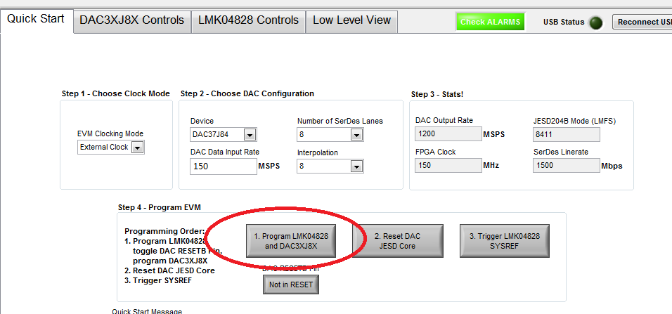
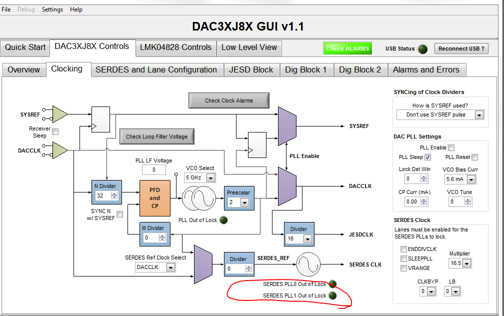
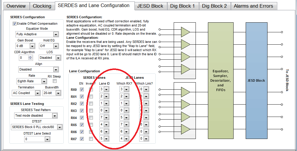
in the SERDES and Lane Configuration interface 

questions 1: LaneID order is 32107465, Which RX? The order is 32105764.Here is correct?What is the correct order?

questions 2:

According to the 0116. DAC38J84 Start - up Sequence of the documentation process configuration (continuous SYSREF), when I read back  the SERDES PLL state(register 0x6C), the value is 0xF00F, PLL unlocked, why?

questions 3:

If I only equipped with 0116. DAC38J84 Start - up Sequence registers of the document mentioned, no other registers configuration, is there a problem?

Now I do it, The output  of DAC is wrong,  At the same time signal of Syncn  changes(high and low). What should I do? The following is a register list .

#include "define.h"
///////////////////////////////////////////////////////////
//////dac37j84
/////////////////////////////////////////////////////////////
u32 DAC37J84_REG_BUFFER[DAC37J84_REG_BUFFER_SIZE]=
{
	0x022081,
	0x022080,
	0x1B0100,
	//------continuous sysref
	0x240000,
	0x5C0000,
	//---5
	0x1A0020,
	0x311000,
	0x320000,
	0x330000,
	//---9
	0x3B0800,
	0x3C8028,
	0x3D0088,
	0x3E0168,
	0x3F0000,
	//---14
	0x461882,
	0x4701C8,
	0x483143,
	0x490000,
	0x4AFF1E,
	0x5F3210,
	0x605764,
	//---21
	0x03A301,
	0x258000,
	
	0x4B1200,
	0x4C1307,
	0x4D0300,
	0x4E0F4F,
	0x4F1C61,
	0x500000,
	0x5100DC,
	0x5200FF,
	0x530000,
	0x5400FC,
	0x5500FF,
	0x560000,
	0x5700FF,
	0x5800FF,
	0x590000,
	0x5A00FF,
	0x5B00FF,
	0x5C1133,
	0x5E0000,
	0x610211,
	
	0x000418,
	0x010003,
	0x022080,
	
	0x080000,
	0x090000,
	0x0A0000,
	0x0B0000,
	0x0C0400,
	0x0D0400,
	0x0E0400,
	0x0F0400,
	0x100000,
	0x110000,
	0x120000,
	0x130000,
	0x140000,
	0x150000,
	0x160000,
	0x170000,
	0x180000,
	0x190000,
	
	0x1E9999,
	0x1F9980,
	0x208008,
	
	0x240030,
	0x5C5555,
	
	0x4AFF1F,
	0x4AFF01
};

Thank you!

  • Liu,

    We will have to look into this and get back to you.

    -Kang
  • Liu,

    1. The default DAC38J84 EVM interfaces with TSW14J56EVM. Due to PCB layout in FMC connector, we have connected the SERDES TX lane from the TSW14J56EVM to the SERDES RX lane on the DAC38J84 EVM with the order of lane #3, 2, 1, 0, 7, 4, 5, 6. These are the SERDES lane number, and they are mapped through our JESD204B RX crossbar/mux to JESD204B lane0, 1, 2,3, 4, 5, 6, 7. For detail, please refer to our EVM schematic and information regarding JESD204B RX input crossbar

    7.3.1.2.4 JESD204B Lane Multiplexer.docx

    2. The SERDES PLL should be locked with default quick-start configuration.

    Note that there is also a on-chip PLL/VCO circuit that provides the DAC sampling clock. You may not necessary be using it, and it is not used by default.

    3. See attached for more detailed start-up sequence:

    8.3 DAC3xJ8x Start-up Sequence.docx

    If the SYNCB LVDS signal is going high and low, this indicates that the JESD204B link is not passing CGS. You may need to work with Xilinx support or look into our TSW14J10 reference code to ensure correct CGS is send.

  • Kang,

    Thanks very much!The SERDES PLL is locked. But there is something wrong with the sync signal.

    In the system, sysref generated by FPGA internal logic. then output to the FPGA jesd_core and dac37j84 chip. as shown, I produced five sysref signal, frequency and LMFC is consistent. when JESD_CORE received the sysref, it start the synchronization process (BCBC character + four frames).

    after receive the sysref Dac37j84 pull the sync is low. JESD_CORE restart a synchronization process to send (BCBC character + four frames), but the sync signal is going high and low, what reason causes this? I still have no idea, you can say some more detailed?  I don't get  TSW14J10 reference code, can you send me a link?

  • Kang,

    In addition,I read back regs ox64-x06B.Values are 0x0001.

    when I set 0x51->0x00F0,0x52->0x00F0,A sync request is not produced. But when I set  0x51->0x00FF,0x52->0x00FF,A sync request is produced.

  • Liu,

    If the LVDS SYNCB is toggling, either the CGS stage or the ILA stage is not passing. The CGS stage involves in K28.5 characters, and the ILA sequence are specific to you JESD204B settings between JESD204B TX and JESD204B RX logic (DAC)

    The DAC38J84 family has an internal build in pattern test for you to verify the CGS stage and ILA stage. See below for test procedure:

    7.3.1.2.5 JESD204B Pattern Test.docx

    See below for ILA sequence configuration check. 

    DAC3xJ8x ILA Sequence.xlsx

    The ILA sequence is described by the following JESD204B standards. It consists of four multi-frame. Each octet is based on the 8bit counter value. You will need to replace certain octets as described in the octet replacement rules. For instance, the 1st octet is always 0x1C, and the last octet is always 0x7C. The 2nd multiframe is where you insert the ILA sequence consist of the JESD204B configuration information in the Excel sheet

    The TSW14j10 EVM website:

    download link.

  • Liu,

    Reading back 0x64 to 0x6B alarm registers to be 0x0001 indicates that the JESD204B TX rate does not match the JESD204B RX rate. I would recommend that you configure the DAC in the DAC GUI in auto programming mode on the main GUI, and then go to the low level page to check each individual registers to confirm the correct setting.

    0x51 are sync request for the JESD204B RX logic. JESD204B requires at a minimum to enable sync request upon 8b/10b disparity and CGS error. Therefore, bit1 and bit3 has to be checked at all time to be 204B compliant.

    -Kang
  • Kang,

    Thank you very much! Now, the DAC output is normal, but I ran into another problem. I want to do two pieces of DAC37J84 synchronization, but output phase is not fixed. I can guarantee to DAC37J84 working clock in phase. what I also need to pay attention to? Any reference document?

  • Liu,

    Here are some discussions regarding multiple DAC37J84 synchronization over JESD204B

    here is a sneak preview to the upcoming TI Design note:

    Published_TIDUBH1_TIDA-00996.pdf

  • Hello! Kang Hsia,
    I bought a DAC38J84EVM and a TSW14J56EVM , now i am debugging my FPGA program on it. I want to ask where can i download the document you and liu talking about ? The document including these chapters such as : 7.3.1.2.4 JESD204B Lane Multiplexer and 7.3.1.2.5 JESD204B Pattern Test ...
    Thank you very much and I am waiting for your help !
  • Hello,

    You should be able to download these documents from the link within the post itself. See the post that I on March 11th, 8:26AM and March 9th.
    -Kang
  • Hello Kang

    Thank you for your replay , I have down load these files, thanks!