Part Number: ADS8685
Support Path: /Product/Development and troubleshooting/Help with board layout or design considerations/
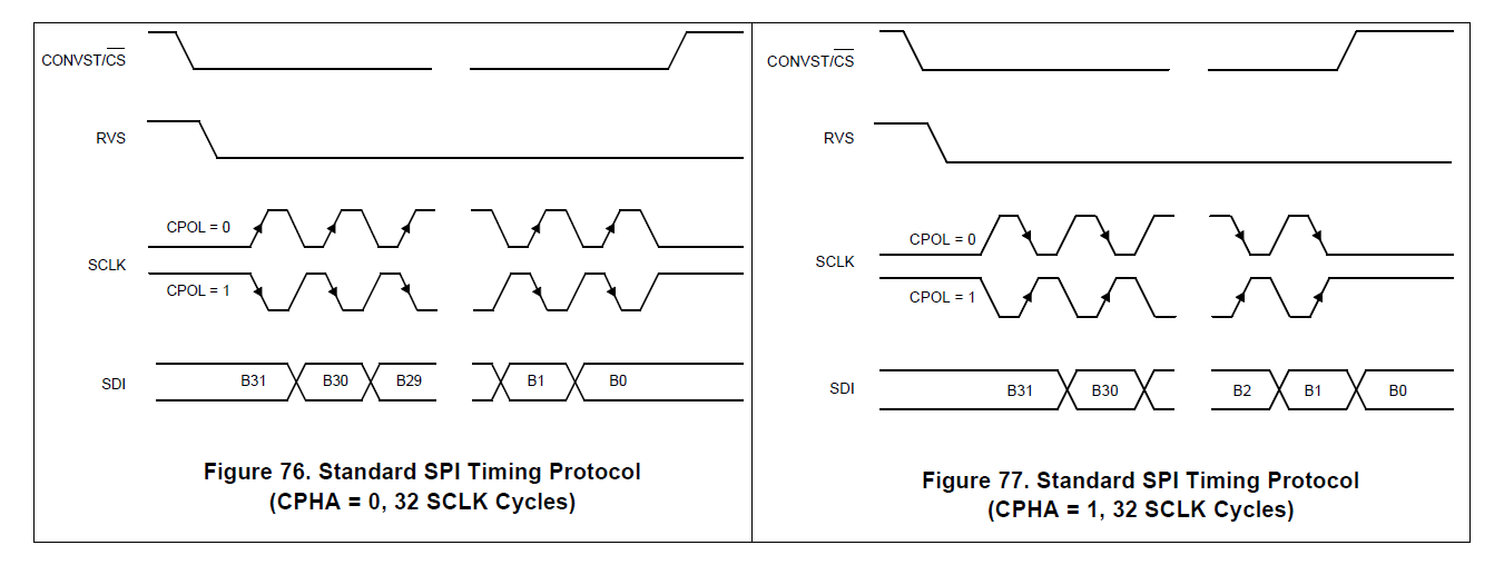
Please I need help understanding the SPI programming protocol of this chip. I want to read and configure registers and read the ADC output data. As the datasheet IS NOT AT ALL EASY TO UNDERSTAND, I need clear examples that show me how to read any Register, write any Register and read the ADC data.
Consider for example my case:
1- I need to know exactly what are the 32 bits that I need to send to READ the RANGE_SEL_REG.
2- I need to know exactly what are the 32 bits that I need to WRITE the RANGE_SEL_REG in order to select de range: +-3 x Vref and Internal Reference.
3- If I use the default protocol as it comes (SPI-00-S), how do I retrieve the ADC data from the chip and how it will be formed (16bits, 32 bits, etc). Do I need to send any Command in order to Read the ADC output data?
4- If I configure the range to +-3 x Vref and Internal Reference, whats the equation to convert the the UNSIGNED INT data to float?
5- Do I have to send all data MSB first? All the data from the chip comes MSB First?
This is my schematic: