This thread has been locked.

If you have a related question, please click the "Ask a related question" button in the top right corner. The newly created question will be automatically linked to this question.

ADS8568: ADS8568 stops responding to CONVST

Part Number: ADS8568

We are observig lockups with ADS8568 operating in SPI modes, which are manifested by devices suddenly stopping to respond to CONVST input with BUSY. Devices operate fine at slower conversion rates (up to 50 ksps) and SCLK speeds (up to 25 MHz), but increasing either results in the device ending up in an unusable state which can only be resolved by asserting the RESET input.

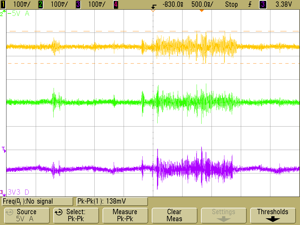
The devices are configured to use the internal conversion clock, and all four CONVST_* inputs are driven by the same input signal. We have designed two boards with ADS8568: on the first one the device is configured for single-line SPI interfacing to an Xilinx Artix-7 FPGA, while the other board uses 4-line SPI readout and is interfaced to an Lattice XP2 FPGA. On both boards DVDD is at 3V3, AVDD and HVDD are at 5V, HVSS is at -5V, p-p jitter of power supplies under load is below 150 mV measured <2cm from the device.

The timing diagram while the device works fine is shown below:

Once we increase the SPI clock to 37.5 MHz, or when we increase the sampling rate without changing the SPI clock, the device stops responding to CONVST input after a few conversion cycles. Applying an input signal apparently speeds up the device lockup, but the device will go belly up even with all 8 analog inputs being tied to GND.

We have tried to both reduce and extend the duration of the CONVST signal, extend the delay from BUSY going low to asserting FS#, extending the delay from asserting FS# to activating the SPI clock, among many other things, to no avail.

Any suggestions on how to further debug this?

  • Hello Marko,

    Thanks for posting this query on E2E. I have few questions:

    1. When ADC stopped responding CONVST signal, also no available BUSY signal which is output was observed, please correct me if my understanding is wrong.

    2. When this happened, what's the data you read during the same stop? repeating the last conversion data? 

    3. When this happened every time, did you get different data same or different data for different stops?

    4. Are you using Hardware or Software mode? 

    ADS8568 can support 480ksps sampling rate for serial interface and 45Mhz SCLK frequency, and should have no problem to support your application. Your schematic will be helpful to address the issue. Before get more information, two tests can be done to check:

    1. increase your HVDD above +5V and reduce HVSS less than -5V, for example, +/-8V or +/-10V, these high voltage power supplies should have wider margins than your maximum input signal(if you want +/-5V input range)

    2. If above 1. doesn't work, please make CONVST high signal longer than BUSY high signal, then check again.

    Thanks.

    Regards

    Dale Li

  • Hi Dale, thanks for looking at this, pls. find comments below:

    Dale Li said:
    1. When ADC stopped responding CONVST signal, also no available BUSY signal which is output was observed, please correct me if my understanding is wrong.

    Exactly, we observe the loss of BUSY response from the ADC.

    Dale Li said:
    2. When this happened, what's the data you read during the same stop? repeating the last conversion data? 

    We have the same analog signal connected to inputs A0 and C0. When BUSY operates normally i.e. per spec sheet, both channels deliver roughly the same reading, differing in only a few least significant bits. When BUSY locks up (remains low after CONVST), A0 readouts remain frozen, but C0 apparently works normally i.e. it follows the analog signal input.

    Dale Li said:
    3. When this happened every time, did you get different data same or different data for different stops?

    Apparently A0 would hold the last value recorded when the ADC operated normally, i.e. we get different A0 readout for different stops. It seems that C0 continues to operate normally.

    Dale Li said:
    4. Are you using Hardware or Software mode? 

    The PCB is hardwired for software mode.

    Dale Li said:
    1. increase your HVDD above +5V and reduce HVSS less than -5V, for example, +/-8V or +/-10V, these high voltage power supplies should have wider margins than your maximum input signal(if you want +/-5V input range)

    I can confirm that fiddling with power supply voltages impacts on the frequency of ADC lockups. The problem is that on our boards HVDD and AVDD are hardwired together so I can only bump the voltage to +/- 6V or so. The higher the voltage, the less lockups we observe.

    Dale Li said:
    2. If above 1. doesn't work, please make CONVST high signal longer than BUSY high signal, then check again.

    Our FPGA logic already guarantees that before CONVST is deasserted the BUSY must return from high to low. We had to modify the FPGA's state machine to ignore the BUSY signal for the experiments I reported above, otherwise it wouldn't proceed to asserting FS# and starting the SPI transfer. We also extended the duration of CONVST from 1.7 to 2.7 us as you suggested, but it didn't make any impact on the stability of ADC operation.

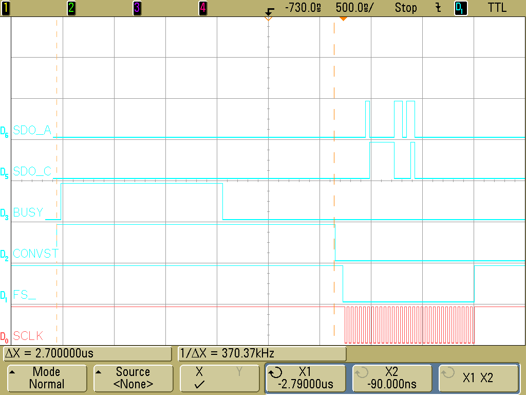
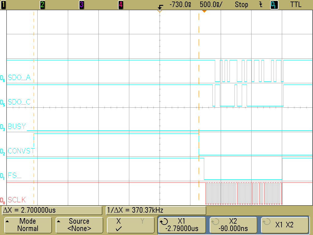
    The two diagrams below are taken with CONVST duration of 2.7 us. On the first one the ADC responds regularly with BUSY, on the second one the absence of BUSY response can be observed.

    Below is the schematic of our development board, nothing spectacular to see here. The signal arriving at input CH_A0 is patched to CH_C0 as well, which is not shown on the schematic. The ADC configuration is determined by attaching (most of) the relevant pins to GND via external jumpers, except SEL_B and SEL_CD which are tied to DVDD.

  • Hello Marko,
    Thanks for detailed feedback, I apologize for late response. Looks like your channel pair A doesn't work, have you configured the Configuration register(CONFIG) after power up? When the HW/SW input is set high, the device operates in software mode with functionality set only by the Configuration register bits. Please make sure PD_x bit = 0 in CONFIG register, check /STBY bit 0 or 1 in CONFIG register. I also suggest to remove R332-R336 resistors for test purpose, /STBY pin to high which should have no impact for SW mode but for test purpose. Thanks.
    By the way, where are SEL_B and SEL_CD you mentioned which are tied to DVDD in schematic?

    Best regards
    Dale Li

  • Hi Dale, thanks for the hints where to look next. I'll be away from the lab for the next 10 days, but as soon as I return I will modify the board per your suggestions, run more tests and post an update here.
  • Hi Dale,

    per your suggestion, we have removed R332-R336 resistors and pulled up the /STBY pin. The device still locks up at higher conversion rates (above 100 ksps), but bemusingly, it now tolerates a 37.5 MHz SPI clock, while in the original setup the chip would lock up immediately once the SPI clock would be increased past 25 MHz.

    SEL_B and SEL_CD are pulled up via external jumpers, not shown on the part of the schematic I posted above.

    The config register is being perpetually updated to 0x800080ff (REF_EN = 1, REFDAC = 0x0ff). There's no way to "check" the status of the config register on ADS8568, since it can be read out only while it is written to. I.e. READ_EN bit (30) only takes effect if WRITE_EN (31) is also enabled, which the datasheet isn't quite clear about.

  • Hi Marko,

    Your value(0x800080ff) is setting all input voltage range to 4 VREF, also you are selecting Internal reference voltage to 2.5 V(Bit 13), so your HVDD and HVSS should be higher than +10V and less than -10V, but you are using +/-5V as HVDD/HVSS power supplies, +/-12V is a good choice for your case(+/-10V range), also D[9:0]: REFDAC setting bits should be set to 0x3FF to get 2.5V reference voltage. Please correct them.
    When Bit 30=1, Configuration register contents output on SDO_A with next two accesses, this is one way to check the register.
    Thanks.

    Regards
    Dale
  • Dale Li said:
    Your value(0x800080ff) is setting all input voltage range to 4 VREF, also you are selecting Internal reference voltage to 2.5 V(Bit 13), so your HVDD and HVSS should be higher than +10V and less than -10V, but you are using +/-5V as HVDD/HVSS power supplies, +/-12V is a good choice for your case(+/-10V range), also D[9:0]: REFDAC setting bits should be set to 0x3FF to get 2.5V reference voltage. Please correct them.

    Hi Dale,

    per your suggestion I've tried fiddling with differend config register setting (0x81a883ff), but the device keeps locking out in the same way as before:

            // (31) Register update enable
            // (24) RANGE_A -> 2 VREF
            // (23) RANGE_B -> 2 VREF
            // (21) RANGE_C -> 2 VREF
            // (19) RANGE_D -> 2 VREF
            // (15) Internal reference enable
            // (9..0) REFDAC setting
            SH(0x81a8, IO_ADC_BASE, ADC_OUT_HI);
            SH(0x83ff, IO_ADC_BASE, ADC_OUT_LO);

    In our application HVDD and HVSS must be tied to +/- 5V, which per the datasheet should be perfectly regular and acceptable values? Or are they not, as you are suggesting we should bump them to +/-10V? Nowhere in the datasheet could I find a hint that +/-10V range on HVDD/HVSS would be a required minimum for using the internal reference voltage generator?

    Furthermore, I do not follow why REFDAC should be fixed to 0x3ff, as per the datasheet the value should be in range from 0.2 VREF to VREF, i.e. from 0x0cc to 0x3ff, or 0.5V to 2.5V?

    Dale Li said:
    When Bit 30=1, Configuration register contents output on SDO_A with next two accesses, this is one way to check the register.

    ?

    I cannot reproduce this. The only way to get the config register value instead of an ADC readout on SDO_A is to set both bits 31 (WRITE_EN) and 30 (READ_EN). If only READ_EN (bit 30) is set SDO_A always tracks analog input.

  • Hi,

    the PAR/SER pin is tied to ground in your schematic. Should be high for serial interface. Make sure RD and REFEN/WR are tied to ground.

    Have you tried to decrease REFDAC ?
  • Lukas Fink said:
    the PAR/SER pin is tied to ground in your schematic. Should be high for serial interface. Make sure RD and REFEN/WR are tied to ground.

    Sure, the PCB has been already modified to tie PAR/SER to the ground, and RD and REFEN/WR are also grounded via external jumpers.

    Lukas Fink said:
    Have you tried to decrease REFDAC ?

    Yes, the chip (mis)behaves identically regardless of the REFDAC setting, from 0x3ff downto 0x0cc, or even lower, though values lower than 0x0cc are outside of the specs.

  • Hello Marko,

    Dale is away on travel for 10 days. Meanwhile, let me try to answer your follow up questions.

    You are correct that HVDD and HVSS can be tied to +/- 5 V. but when the previous configuration you were using was indicating using a range from 4*Vref (no matter if internat or external reference is used), thus if internal Vref = 2.5V is used, the input range is 4*2.5 = 10V. This is why Dale explained that you may change the supply voltage, or change the configuration settings to use the smaller range of 2*Vref = 5V.

    As for the last bits being set to 0x3FF, this is the default value. The reference feeds a 10-bit DAC controlled by these REFDAC[0:9] bits. If you wish to use a different configuration, please look at Equation3 on page 31 on the datasheet.

    I do belive you will need to set both Bit 31 and bit 30 to high to be able to read the configuration contents. when you set the configuration register, are you seeing configuration data you just have programmed on SDOA? 

    To confirm, what communications interface are you using, serial or parallel?

    Regards, Cynthia

  • Hi Cynthia,

    we are using SPI only as stated at the beginning of this thread. The schematic I posted above is for our homebrew evaluation board, which was originally intended for parallel communication, but we patched it up for quad-SPI by rewiring PAR/SER to DVDD. In my previous reply to Lukas Fink I've incorrectly stated that PAR/SER was patched to GND, but in fact we removed R329 and wired the pin directly to DVDD.

    While it wouldn't be unexpected to see erratic behavior on a patched-up evaluation board full of jumpers, we are worried as we have another board, which I'm not at the liberty of posting the schematic of here, which was from the outset designed and routed for single-SPI operation. We are observing exactly the same lockups there with single-readout SPI as we are experiencing on our evaluation board with quad-readout SPI, once we bump the conversion rate from around 50 ksps up.

    Initially we blamed the lockups to noisy power supplies but we are no longer convinced they are the culprit. Depending of the conversion rate, we are observing between 40 and 55 mA average current consumption on the +5V power rail (from which 3V3 DVDD is also derived through a LDO), with voltage spikes of no more than 150 mV measured less than an inch from the ADS8568 chip, as can be seen on the oscillogram I posted here earlier.