This thread has been locked.

If you have a related question, please click the "Ask a related question" button in the top right corner. The newly created question will be automatically linked to this question.

ADS1255: ADS1255 PSEUDO DIFFERENTIAL CONFIGURATION

Part Number: ADS1255
Other Parts Discussed in Thread: THS4551, , TLV333

Dear All

5305.Schematic Prints.pdf

Schematic its attached, please, see

I removed THS4551 (Fully differential Coniguration)

Now i need to proceed with Pseudo Differential Configuration

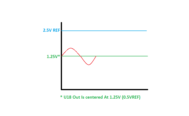
U18 Output is centered at 1.25V VCOM (0.5VRef), VREF is 2.50 V

Should I connect ADC_IN_N to AGND or To VCOM?

Should I connect AINCOM to AGND or To VCOM?

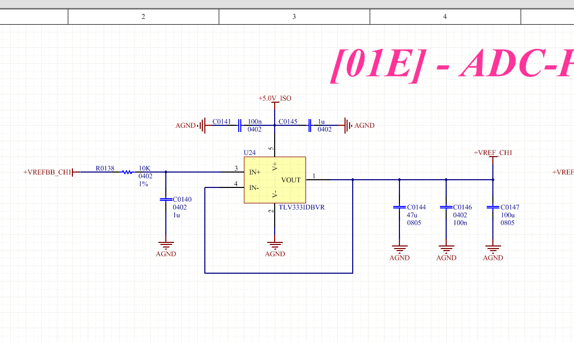
PD: Vref its buffered in another schematic sheet
  • ADS1255 Outputs Twos Complement Code

    So i thing its better to tie in_n to vref/2 (vcom), instead of ground, in this way i avoid the noisy ground

    vref/2 (vcom) takes advantage of 5V LDOpsrr + ref5025psrr+tlv333(u17)psrr

    So IN_N will be much less noisy

    Right?
  • Schematic remains as follows (Schematic Prints2)

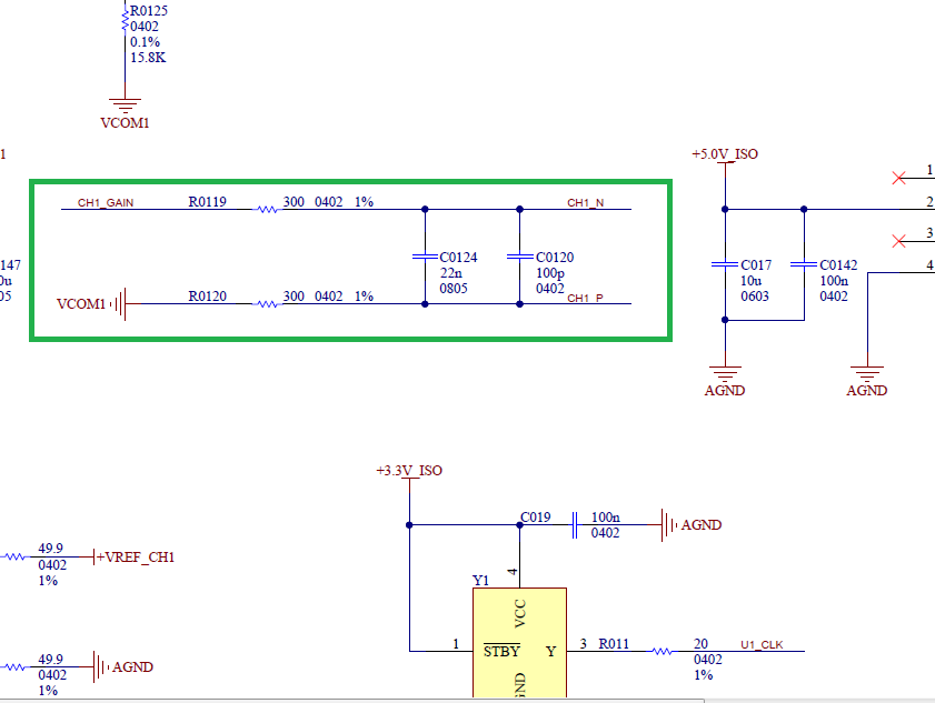
    What is optimal value for passive RC 15Khz for full accuracy, Clk 8Mhz, Sampling at 30.khz

    Schematic Prints2.pdf

  • Ignacio,


    As I'd mentioned in the previous post, I would tie the negative input to the 1.25V node. It allows you to put the device in gain and not have a 1.25V DC offset for the measurement. However, this does have some risk. Note that your 1.25V source has some error associated with it. If the voltage divider is perfect, the error is going to be half of the initial accuracy error from the REF5025. Second, your divider is made up of 1% resistors, which means that the divider error could be up to 2% off from the expected value. If this error is important or it cannot be calibrated out, then maybe attaching the negative input to this 1.25V isn't a good idea. Again, I don't know what it is you are measuring, so I don't know if this a problem for you.

    Note, most of the time we think of the ground as a clean analog node, not a noisy ground. Often, we talk about laying out separate analog and digital grounds, but it's best to think of the ground as a clean node. Then lay out the board so that the ground is as clean as possible. Below is a link to a discussion about ground planes.

    e2e.ti.com/.../1393

    For the input filtering of the ADS1255, if you're using a data rate of 30kSPS, I would use a filter bandwidth of greater than 30kHz, not less than 30kHz. There are two things to consider. If you're not using the buffer, the series resistance will react with the input current to cause an error. In high PGA gain, this input current is larger. In general you'll want to keep this resistance as a lower value. Second, the filter capacitor acts as a charge bucket for the sampling process. If you used something like two 50Ω series resistances, with a 22nF capacitor, it would probably be fine.


    Joseph Wu