This thread has been locked.

If you have a related question, please click the "Ask a related question" button in the top right corner. The newly created question will be automatically linked to this question.

About "Read DDR to file" error in HSDC pro software for tsw14j56 product

Other Parts Discussed in Thread: ADS54J69, ADS54J69EVM

Hi,
I got errors about "Read DDR to file" in HSDC pro software. The error message shows "Timed_OUT_ERROR".

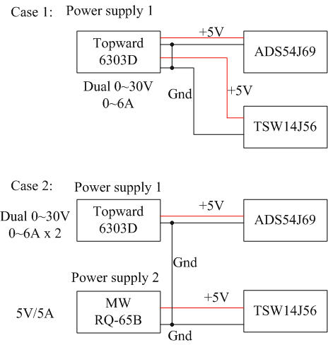
My hardware are:  Adc board is ads54j69   &  Fpga board is tsw14j56.


My HSDC pro setting are:
The sampling frequency is 491.52MHz, Sample point is 65536
the function generator is set 10MHZ, Ro=50ohm, amp=0.3vpp, bias=0.15v. 

I had checked led status in fpga board in which D4 led is blinking,  D3 led is off.  and ADC PLL2 lock (D2 led is on).
The setting file of the Adc board are LMK_Config_Onboard_983p04_MSPS and ADS54J69_2x_dec_lowpass. 

How can i solve this timed out error?   this problem confuses me about one week. 
Many thanks for the help. 

  • The error log are shown :
    ------------------------------------------------------------------------------------------------------------------------
    Error code : 102.000000
    Error Description:
    Read DDR to file
    TIMED_OUT_ERROR
    Possible reasons for Time Out Error:
    1.FPGA may be in reset.
    2.Clock from ADC EVM is not received by TSW Board. Please check if D4 LED is blinking. 3.SYNC is not established between ADC and FPGA. Please check if D3 LED is OFF. Possible reasons for SYNC Failure: a.JESD Ref clock Input Frequency to the TSW board from ADC EVM is not correct. b.JESD configuration is not same in ADC and the INI file selected.
    ADC/DAC name : ADS54J69_2x_4222
    IID: 3.000000
    Device config details:

    [ADC]

    Interface name="TSW14J56REVD_FIRMWARE"
    Number of channels=2
    \\Channel Pattern=1-2,2-2,1-4,2-4,1-6,2-6,1-8,2-8,1-1,2-1,1-3,2-3,1-5,2-5,1-7,2-7
    Channel Pattern=1-2,1-4,1-1,1-3,2-2,2-4,2-1,2-3,1-6,1-8,1-5,1-7,2-6,2-8,2-5,2-7
    Data Postprocessing=1:32768
    \\operation:operand
    \\operaion
    \\0=bit shift
    \\1=xor
    \\2=and
    \\3=or
    \\4=not
    \\operand
    \\value(+ve if bitshift by right and -ve if bitshift by left)
    \\E.g 0:-2,1:1024
    \\bitshift by left 2 times and then xor by 1024
    Number of Bits=16
    Max sample Rate=500000000
    Register_Config="-"
    \\[Register Address]:[Register Value]:[Number of Bytes to be sent as]
    DLL Version=1.0
    Read EVM Setup Procedure="EVM Setup Procedure not available"
    \\use <> as delimiter for newline

    [Version 1.0]

    JESD IP Core_CS=0
    JESD IP Core_F=2
    JESD IP Core_HD=0
    JESD IP Core_K=16
    JESD IP Core_L=4
    JESD IP Core_M=4
    JESD IP Core_N=16
    JESD IP Core_NTotal=16
    JESD IP Core_S=1
    JESD IP Core_SCR=0
    JESD IP Core_Tailbits=0
    JESD IP Core_LaneSync=1
    JESD IP Core_Subclass=1
    JESD IP Core_JESDV=1
    MIF Config= 0.611G to 1.5G:RX:RX_PMA_x10,1.5G to 5.125G:RX:RX_PMA_x20
    \\List of Lane Rate Range,PLL Type and their MIF File names that needs to be configured,separated by ":"
    \\These MIF Files need to be present under MIF Files Folder
    Fabric PLL Counter = 0.611G to 1.5G:0x080808,1.5G to 5.125G:0x080404
    Invert Sync Polarity = 0
    \\Invert Sync polarity, 1:invert; 0: do not invert
    Invert Serdes Data = 0
    \\Invert Serdes Data, 1:invert; 0: do not invert
    Transceiver Mode = 0
    \\1:xcvr mode; 0: TX/RX only mode
    Lane Mapping=lane0:7,lane1:4,lane2:3,lane3:0
    \\Lane pattern for the LMF modes
    Group 128 bits Flag = 1
    \\If 1, will group 128 bits from each DDR, and then apply the channel pattern
  • HY,

    Make sure the 5V power supply connected to the TSW14J56EVM is capable of providing at least 3A. If this supply is also connected to the ADC EVM, make sure it can provide at least 5A. After you load the LMK_Config_Onboard_983p04_MSPS file, press the reset switch on the ADC board before loading the ADC config file.

    Regards,

    Jim  

  • Hi, Jim

    The connect of the power supply to ADC board and FPGA board are shown below.

    I try two cases about power supply connection.

    The operational procedure are:

    0. connect usb cables and power cables of ADC board and FPGA, respectively.

    1. TSW14J56EVM
     1.1: power on
     1.2: turn on "sw6"

    2.ADS54J69EVM
     2.1: load clock configuration file  ==> 983p04_MSPS.cfg,
     2.2: after PLL2 LED on
     2.3  press "SW1" for  ADC RESET
     2.4: load adc configuration file ==> ADS54J69_2x_dec_lowpass_4222.cfg

    HSDC PRO also shows the same error message as posted message

    Operating System Name : Windows 7 Enterprise 32 bit Service Pack 1
    Error code : 102.000000
    Error Description: 
    Read DDR to file
    TIMED_OUT_ERROR
    Possible reasons for Time Out Error:     
    1.FPGA may be in reset.
    2.Clock from ADC EVM is not received by TSW Board. Please check if D4 LED is blinking.
    3.SYNC is not established between ADC and FPGA. Please check if D3 LED is OFF. 
    Possible reasons for SYNC Failure:               
    a.JESD Ref clock Input Frequency to the TSW board from ADC EVM is not correct.  
    b.JESD configuration is not same in ADC and the INI file selected.
    ADC/DAC name : ADS54J69_2x_4222
    IID: 3.000000
    Device config details:
    
    [ADC]
    
    Interface name="TSW14J56REVD_FIRMWARE"
    Number of channels=2
    \\Channel Pattern=1-2,2-2,1-4,2-4,1-6,2-6,1-8,2-8,1-1,2-1,1-3,2-3,1-5,2-5,1-7,2-7
    Channel Pattern=1-2,1-4,1-1,1-3,2-2,2-4,2-1,2-3,1-6,1-8,1-5,1-7,2-6,2-8,2-5,2-7
    Data Postprocessing=1:32768
    \\operation:operand
    \\operaion
    \\0=bit shift
    \\1=xor
    \\2=and
    \\3=or
    \\4=not
    \\operand
    \\value(+ve if bitshift by right and -ve if bitshift by left)
    \\E.g 0:-2,1:1024
    \\bitshift by left 2 times and then xor by 1024
    Number of Bits=16
    Max sample Rate=500000000
    Register_Config="-"
    \\[Register Address]:[Register Value]:[Number of Bytes to be sent as]
    DLL Version=1.0
    Read EVM Setup Procedure="EVM Setup Procedure not available"
    \\use <> as delimiter for newline
    
    [Version 1.0]
    
    JESD IP Core_CS=0
    JESD IP Core_F=2
    JESD IP Core_HD=0
    JESD IP Core_K=16
    JESD IP Core_L=4
    JESD IP Core_M=4
    JESD IP Core_N=16
    JESD IP Core_NTotal=16
    JESD IP Core_S=1
    JESD IP Core_SCR=0
    JESD IP Core_Tailbits=0
    JESD IP Core_LaneSync=1
    JESD IP Core_Subclass=1
    JESD IP Core_JESDV=1
    MIF Config= 0.611G to 1.5G:RX:RX_PMA_x10,1.5G to 5.125G:RX:RX_PMA_x20
    \\List of Lane Rate Range,PLL Type and their MIF File names that needs to be configured,separated by ":"
    \\These MIF Files need to be present under MIF Files Folder
    Fabric PLL Counter = 0.611G to 1.5G:0x080808,1.5G to 5.125G:0x080404
    Invert Sync Polarity = 0 
    \\Invert Sync polarity, 1:invert; 0: do not invert
    Invert Serdes Data = 0  
    \\Invert Serdes Data, 1:invert; 0: do not invert
    Transceiver Mode = 0  
    \\1:xcvr mode; 0: TX/RX only mode
    Lane Mapping=lane0:7,lane1:4,lane2:3,lane3:0
    \\Lane pattern for the LMF modes
    Group 128 bits Flag = 1
    \\If 1, will group 128 bits from each DDR, and then apply the channel pattern

  • HY,

    In case the config files you are using got corrupted, please try the config files attached as I just tested these with our hardware. The TSW14J56EVM .ini file needs to go in the following location:

    C:\Program Files(86)\Texas Instruments\High Speed Data Converter Pro\14J56revD Details\ADC files.

    If this does not work, try the 4x example in the ADS54J69EVM User's Guide. You will need to copy the "ADS54J69_4x_2221.ini file into the location mentioned earlier in this post. If this does not work, contact your distributor to request for an exchange of the ADS54J69EVM. I am not sure which board could be causing this issue but lets start with the ADC EVM first if an exchange is required.

    Regards,

    Jim 

    ADS54J69_2x_dec_lowpass.cfghttps://e2e.ti.com/cfs-file/__key/communityserver-discussions-components-files/73/ADS54J69_5F00_4x_5F00_2221.inihttps://e2e.ti.com/cfs-file/__key/communityserver-discussions-components-files/73/ADS54J69_5F00_2x_5F00_4222.ini

  • Hi  Jim

    Thank you for providing the files to test. The same error message, Read DDR to file, is shown again.

    I wrote down the LED status of the ADC board and the FPGA board.

    The same cases were also happened in 

    How can i do for this situation ? 

  • Hi Jim,
    I have an another new ADC board(ads54j69) . After test with FPGA board( tsw14j56). The same error message is shown.
    I think that FPGA board is fail.
    Could i send the serial number of FPGA board to you for exchanging the FPGA board?
    Many thanks for your help.
  • HY,

    Work with your distributor on getting a replacement. Let me know if they require any other information from us to get you this new board.

    Regards,

    Jim 

  • Hi. Jim

    OK,  Many thanks for your supports.

    Regards,

    HY