


Tool/software: Code Composer Studio
I have designed a Launchpad shield for use with 6 load cells but am having issues with getting the SPI interface to function correctly.
I am using the UCB1 SPI pins available on the Launchpad
P5.0 UCB1SIMO
P5.1 UCB1SOMI
P5.2 UCB1CLK
The following code worked well in communicating with a DS3234 RTC but has been modified to get the correct Polarity and Phase for the ADS124S08
#include <driverlib.h>
unsigned char spiTransferB1(unsigned char writeData)
{
while (!(UCB1IFG & UCTXIFG)); // wait for TX buffer ready
UCB1TXBUF = writeData;
while (!(UCB1IFG & UCRXIFG)); // wait for RX buffer ready
return UCB1RXBUF;
}
void Init_SPI(void)
{
EUSCI_B_SPI_disable(EUSCI_B1_BASE); // disable the EUSCI to be programmed.. ie set the UCSWRST bit
GPIO_setAsPeripheralModuleFunctionOutputPin(GPIO_PORT_P5,GPIO_PIN0,GPIO_PRIMARY_MODULE_FUNCTION);
// Select Port 5, Set Pin 0 to output Primary Module Function, (UCB1TXD/UCB1SIMO)
GPIO_setAsPeripheralModuleFunctionOutputPin(GPIO_PORT_P5,GPIO_PIN2,GPIO_PRIMARY_MODULE_FUNCTION);
// Set port 5, Pin 2 to output Primary Module Function, UCB1CLK.
GPIO_setAsPeripheralModuleFunctionInputPin(GPIO_PORT_P5,GPIO_PIN1,GPIO_PRIMARY_MODULE_FUNCTION);
// Select Port 5, Set Pin 1 to input Primary Module Function, ( UCB1RXD/UCB1SOMI)
// Disable the GPIO power-on default high-impedance mode to activate previously configured port settings
PMM_unlockLPM5();
//Initialize UCB1 as SPI Master -- debugging SPI for TI ADS124S08
EUSCI_B_SPI_initMasterParam param = {0}; // param is struct data type
param.selectClockSource = EUSCI_B_SPI_CLOCKSOURCE_SMCLK;
param.clockSourceFrequency = 1000000; // note SCLK out is half of source clock >> SCLK will be 4MHz which is max for DS3234
param.desiredSpiClock = 1000000;
param.msbFirst = EUSCI_B_SPI_MSB_FIRST;
param.clockPhase = EUSCI_B_SPI_PHASE_DATA_CAPTURED_ONFIRST_CHANGED_ON_NEXT; // <<< for ADC Require Ph = 1, For RTC require Ph = 0
param.clockPolarity = EUSCI_B_SPI_CLOCKPOLARITY_INACTIVITY_LOW; // Low for ADC, Pol = 0; High for RTC Pol = 1
param.spiMode = EUSCI_B_SPI_3PIN;
EUSCI_B_SPI_initMaster(EUSCI_B1_BASE, ¶m); // *** B SPI is initialised with struct param data
//Wait for lines to stabilise prior to switching on the SPI
__delay_cycles(100);
//Enable SPI module
EUSCI_B_SPI_enable(EUSCI_B1_BASE); // clear the UCSWRST bit to enable the SPI
EUSCI_B_SPI_clearInterrupt(EUSCI_B1_BASE,EUSCI_B_SPI_RECEIVE_INTERRUPT);
// Enable USCI_B1 RX interrupt
EUSCI_B_SPI_enableInterrupt(EUSCI_B1_BASE,EUSCI_B_SPI_RECEIVE_INTERRUPT);
GPIO_setOutputHighOnPin(GPIO_PORT_P5,GPIO_PIN7); // disable RTC chip
GPIO_setAsOutputPin(GPIO_PORT_P5,GPIO_PIN7); // Set P5.7 as output pin for CS of RTC
GPIO_setOutputHighOnPin(GPIO_PORT_P4,GPIO_PIN3); // disable ADC chip
GPIO_setAsOutputPin(GPIO_PORT_P4,GPIO_PIN3); // Set P4.3 as output pin for CS of ADC
//Wait for slave to initialize
__delay_cycles(100);
}
********************************************************************
I am using the following I/O ports for the ADS124S08 chip...
P4.1 START_SYNC
P4.2 DRDY (Data Ready)
P4.3 CS
#include "driverlib.h"
#include "SigDelta_6ch_ADC.h"
#include "seatPost.h"

extern uint8_t ADC_Status;

void Init_ADC_IO(void)
{
    /**********************************************************************************************
     *                               PORT 4<1~3> used for control lines on ADC chip
           P4.1 is START_SYNC           P4.2 is DRDY_N             4.3 is  CS_N (chip select)
     ************************************************************************************************/
    GPIO_setOutputLowOnPin(GPIO_PORT_P4,GPIO_PIN1);  // Set P4.1 output Low -  Active High pin starts conversion [START_SYNC]
    GPIO_setAsOutputPin(GPIO_PORT_P4,GPIO_PIN1);     // ADC START/SYNC low for ADC start via commands; active High for continuous conversions
    GPIO_setAsInputPin(GPIO_PORT_P4,GPIO_PIN2);      // Set P4.2 as ADC Data Ready signal
    GPIO_setOutputHighOnPin(GPIO_PORT_P4,GPIO_PIN3);  // Set P4.3 output High - deselect ADC
    GPIO_setAsOutputPin(GPIO_PORT_P4,GPIO_PIN3);     // ADC Chip Select - for SPI communication
}

uint8_t ADC_Setup(void)
{
    GPIO_setOutputLowOnPin(GPIO_PORT_P4,GPIO_PIN3);  // Set P4.3 output Low - select ADC
    __delay_cycles(1);             // delay for minimum td (CSSC)  20nS minimum
                                    // note @4MHz clk, 1 cycle = 250nS
    spiTransferB1(0x06);            // RESET command sent 0x06
    __delay_cycles(4096);           // delay for settling ADC

    do {
        spiTransferB1(0x21);            // read Register starting at REG 1 - STATUS
        spiTransferB1(0x00);            // read 1 register only - which is the Status Reg
        ADC_Status = spiTransferB1(0x00); // read the status data here
       } while (ADC_Status && 0x40)
       ;   // wait for !RDY to go High  (!RDY goes Lo)


    spiTransferB1(0x41);    // write to status register
    spiTransferB1(0);       // write to only 1 reg
    spiTransferB1(0x00);    // Optional   clear the FL_POR flag here
    GPIO_setOutputHighOnPin(GPIO_PORT_P4,GPIO_PIN3);  // Set P4.3 output High - deselect ADC
//    P4OUT |= 0x08;          // Set ADC CS pin high (P4.3)

    return 0;
}

void ADC_Test(void)
{
    //  ADC_Setup follows
    extern unsigned char Mux_Channels;
    extern unsigned char Data_Rate;

    GPIO_setOutputLowOnPin(GPIO_PORT_P4,GPIO_PIN3);  // Set P4.3 output Low - select ADC
   __delay_cycles(1);               // delay for minimum td (CSSC)  20nS minimum
                                    // note @1MHz clk, 1 cycle = 1uS
    spiTransferB1(0x06);            // RESET command sent 0x06
    __delay_cycles(4096);           // delay for settling ADC td(RSSC) = 4096 tclk  (4.096mS using 1MHz SMCLK)

    spiTransferB1(0x21);            // read Register starting at REG 1 - STATUS
    spiTransferB1(0x00);            // read 1 register only -

    ADC_Status = spiTransferB1(0x00); // read the status data here

    spiTransferB1(0x41);            // write to status register
    spiTransferB1(0x00);            // write to only 1 reg
    spiTransferB1(0x00);            // clear the FL_POR flag here - Optional

    /*****************************************************
     *  Write to ADC registers to configure device here
     *****************************************************/
    spiTransferB1(0x42);            // write register WREG starting at REG adr 0x02 (Mux Pair)
    spiTransferB1(0x03);            // <03> write to 4 consecutive registers ( 2,3,4 and 5) [#regs - 1]
    spiTransferB1(0x01);            // write to register 0x02: Select MUX pair  Channel eg Ch0 + , Ch1 - will be 0x01
    spiTransferB1(0x0F);            // write to register 0x03: PGA Gain = 128, delay = 14 t(MOD)
    spiTransferB1(0x15);            //  0x15 = 50 sps, write to register 0x04: Data Rate2000 sps, continuous conversion (0x1C)  for 2000 sps single shot conversion, (0x3C)
    spiTransferB1(0x30);            // write to register 0x05: REFSEL = REFP0, REFN0, Disable Buffers, Internal reference off

    spiTransferB1(0x49);            // Sys Monitor to normal input mode [0x09] SYS_ADDR_MASK
    spiTransferB1(0x00);            // WREG 1 register only
    spiTransferB1(0x10);            // SYS Mon disabled,8 cal samples, timeout disabled, CC disabled, SENDSTAT disabled

    /*********************************
     *  Read back register info here
     *********************************/
    spiTransferB1(0x22);            // Read register RREG starting at REG adr 0x02 (Mux Pair)
    spiTransferB1(0x01);            // Read 2 consecutive registers ( 2,3 [#regs - 1]
    Mux_Channels = spiTransferB1(0x00);  // Read register 0x02: Select MUX pair  Channel eg Ch0 + , Ch1 - will be 0x01
    Data_Rate = spiTransferB1(0x00);     // Read register 0x03: PGA Gain = 128, delay = 14 t(MOD)

    GPIO_setOutputHighOnPin(GPIO_PORT_P4,GPIO_PIN3);  // Set P4.3 output High - deselect ADC
}
In my main loop I initialise all the hardware and then drop into LPM4 and use a 1 second timer to service my routines.
In the main loop code below, I have disabled the RTC code and have only the ADC chip operating on the UCB1 SPI bus to debug.
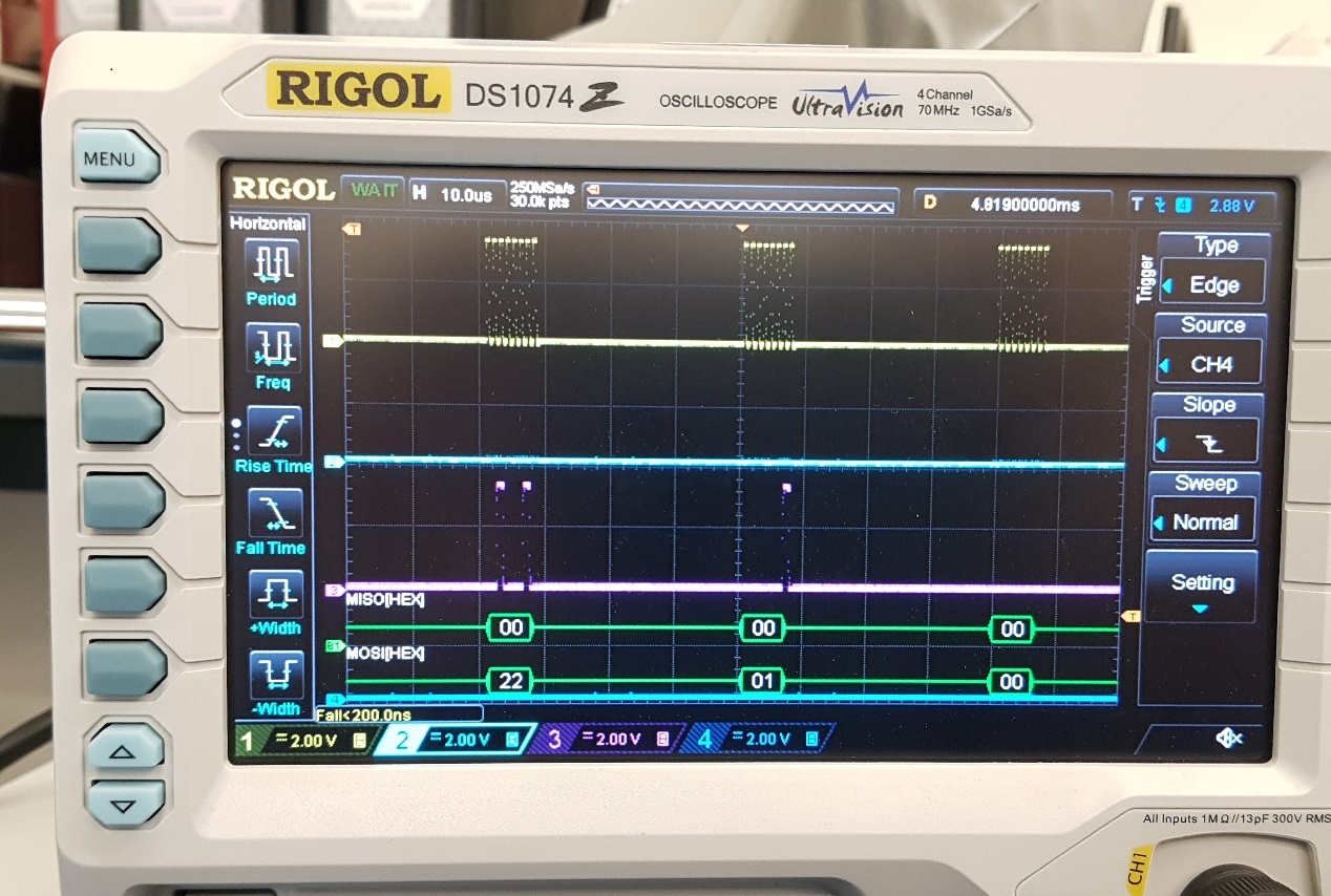
I am having issues with basic reading of the Registers in the ADC_Test() function call.
I can see the transmit data appearing on a scope (P5.0), but am not receiving any data on SOMI P5.1
CH 1 is SCLK CH 2 is SOMI, Ch 3 is SIMO Ch4 is CS,
This is image relates to code in ADC_Test() where the MUX_Channel and Data_Rate registers are read. Been battling this for a while with no success.
Hoping it's something simple I have overlooked.
#define COMPARE_VALUE 200    // 200 for debug @ 1MHz.  Use 800 for 4MHz normal use
//  COMPARE_VALUE sets time-base for TIMER1_A0    If using MCLK = 4MHz     800 x 0.25uS = 0.0002 sec  >>>  5 kHz rate
//  COMPARE_VALUE sets time-base for TIMER1_A0    If using MCLK = 1MHz     200 x 1uS = 0.0002 sec  >>>  5 kHz rate
#include "driverlib.h"
#include "SeatPost.h"
#include "RTC_DS3234.h"
#include "SigDelta_6ch_ADC.h"


void USCI_B1_ISR(void);


unsigned char Mux_Channels = 0;
unsigned char Data_Rate = 0;
unsigned char RXData = 0;
unsigned char TXData = 0;
unsigned char seconds, minutes, hours, day, date, month_century, year;
uint8_t ADC_Status = 0x00;  //set ADC !RDY bit high as Not Ready


struct RTC RTC; // global declaration of RTC structure
uint32_t load = 0x00000000;
int n = 1;
int i = 1;
int storeTime = 0;
uint8_t ADC_OK = 0;

void InitHardware(void)
{
       //   RED LED on Launchpad, uses P1.0  (active Lo). __delay_cycles(500000) produces 1 second period with  500kHz clk
       GPIO_setOutputLowOnPin(GPIO_PORT_P1,GPIO_PIN0);  // Set P1.0 output Low
       GPIO_setAsOutputPin(GPIO_PORT_P1,GPIO_PIN0);     // Red Led indicator for SD Card error!

       GPIO_setOutputLowOnPin(GPIO_PORT_P1,GPIO_PIN1);  //Set P1.1 as Output Low.
       GPIO_setAsOutputPin(GPIO_PORT_P1,GPIO_PIN1);     //Set P1.1 as an output pin. - Green Led for testing GPIO and checking clock freq.....

       GPIO_setAsInputPin(GPIO_PORT_P7,GPIO_PIN2);      // Set P7.2 as SD Card detect port....  Launchpad port allocation P7.2
}

 void InitClkSource(void)
{   //  change to 4MHz for debugging, DCOFSEL_0
//     CS_setDCOFreq(CS_DCORSEL_0,CS_DCOFSEL_3);   //Set DCO frequency to 4000000 MHz setting  ( Low freq (CS_DCORSEL_0) option of DCOFSEL_3 )
//     CS_initClockSignal(CS_SMCLK,CS_DCOCLK_SELECT,CS_CLOCK_DIVIDER_1);    // Set SMCLK = DCO with frequency divider of 1
//     CS_initClockSignal(CS_MCLK, CS_DCOCLK_SELECT, CS_CLOCK_DIVIDER_1);  // Set MCLK = DCO with frequency divider of 1

     //  for debugging, have reduced clock to 1MHz
     CS_setDCOFreq(CS_DCORSEL_0,CS_DCOFSEL_0);   //Set DCO frequency to 1000000 MHz setting  ( Low freq (CS_DCORSEL_0) option of DCOFSEL_0 )
     CS_initClockSignal(CS_SMCLK,CS_DCOCLK_SELECT,CS_CLOCK_DIVIDER_1);    // Set SMCLK = DCO with frequency divider of 1
     CS_initClockSignal(CS_MCLK, CS_DCOCLK_SELECT, CS_CLOCK_DIVIDER_1);  // Set MCLK = DCO with frequency divider of 1
}

 void Init_Timer(void)
 {
     Timer_A_initContinuousModeParam initContParam = {0};    //Start timer in continuous mode sourced by SMCLK
     initContParam.clockSource = TIMER_A_CLOCKSOURCE_SMCLK;
     initContParam.clockSourceDivider = TIMER_A_CLOCKSOURCE_DIVIDER_1;
     initContParam.timerInterruptEnable_TAIE = TIMER_A_TAIE_INTERRUPT_DISABLE;
     initContParam.timerClear = TIMER_A_DO_CLEAR;
     initContParam.startTimer = false;
     Timer_A_initContinuousMode(TIMER_A1_BASE, &initContParam);

     Timer_A_clearCaptureCompareInterrupt(TIMER_A1_BASE, TIMER_A_CAPTURECOMPARE_REGISTER_0); //Initialize compare mode
     Timer_A_initCompareModeParam initCompParam = {0};
     initCompParam.compareRegister = TIMER_A_CAPTURECOMPARE_REGISTER_0;
     initCompParam.compareInterruptEnable = TIMER_A_CAPTURECOMPARE_INTERRUPT_ENABLE;
     initCompParam.compareOutputMode = TIMER_A_OUTPUTMODE_OUTBITVALUE;
     initCompParam.compareValue = COMPARE_VALUE;
     Timer_A_initCompareMode(TIMER_A1_BASE, &initCompParam);
     Timer_A_startCounter(TIMER_A1_BASE, TIMER_A_CONTINUOUS_MODE);
 }


void Test_RTC_Read(void)
{
    hours = RTC.Hours;
    minutes = RTC.Minutes;
    seconds = RTC.Seconds;

    day = RTC.DayOfMonth;
}


void main(void)
{
    volatile uint16_t i;

    __delay_cycles(8800);   // delay 2.2 ms to allow power supplies to reach minimum operating levels


    //Stop watchdog timer
    WDT_A_hold(WDT_A_BASE);

    InitHardware();
    InitClkSource();
    Init_Timer();
    Init_SPI();
    Init_ADC_IO();
    ADC_Setup();
    GPIO_setOutputLowOnPin(GPIO_PORT_P1,GPIO_PIN0);     // Red Led Off
    GPIO_setOutputLowOnPin(GPIO_PORT_P1,GPIO_PIN1);     // Green Led Off


    /*********************************************************************
 *     Call    RTC_Set()  function to set the time                   *
 ********************************************************************/
//   RTC_Set();     // remove comment operator at start of this line to enable the RTC_Set() function
                    //  You must define the current date and time parameters in the RTC_DS3234.h file

    GPIO_toggleOutputOnPin(GPIO_PORT_P1,GPIO_PIN0); // Toggle the Red Led  (toggle ON on first call)

      __bis_SR_register(LPM4_bits + GIE); //Enter LPM4 enable interrupts
      __no_operation();       //For debugger
}


// TIMER1_A3 interrupt vector service routine.  set as 5kHz interrupt service
/*    Interrupt Service Routine below is where all call functions are placed
 *    to read sensors and perform calcs and output data            etc.  */


#if defined(__TI_COMPILER_VERSION__) || defined(__IAR_SYSTEMS_ICC__)
#pragma vector=TIMER1_A0_VECTOR
__interrupt
#elif defined(__GNUC__)
__attribute__((interrupt(TIMER1_A0_VECTOR)))
#endif

void TIMER1_A0_ISR(void)
{

    uint16_t compVal = Timer_A_getCaptureCompareCount(TIMER_A1_BASE,TIMER_A_CAPTURECOMPARE_REGISTER_0) + COMPARE_VALUE;

    if  (n != 5000)         // Cycles 4,999 times
                n++;        //       will be used to capture data every 5000th cycle  (5kHz rate)
    else
        {   // every 5000 cycles (@ 5kHz) will be every 1 second, perform the following
             n = 1;
             GPIO_toggleOutputOnPin(GPIO_PORT_P1,GPIO_PIN1);      // Toggle Green RUN LED (P1.1)
             ADC_Test();
//           RTC_Read();    // Read Real Time Clock and update global structure RTC (struct type RTC)
//           load = ADC_Read(0x01); // read MUX pair Ch 0:1

             if (!SDCard_Detect())
                     GPIO_setOutputLowOnPin(GPIO_PORT_P1,GPIO_PIN0);    // Turn Red Led Off if SD card OK
             else   GPIO_setOutputHighOnPin(GPIO_PORT_P1,GPIO_PIN0);    // Turn Red Led ON if SD card is missing
        }
    i++;
    Timer_A_setCompareValue(TIMER_A1_BASE,TIMER_A_CAPTURECOMPARE_REGISTER_0,compVal);  //Add Offset to CCR0
}


