This thread has been locked.

If you have a related question, please click the "Ask a related question" button in the top right corner. The newly created question will be automatically linked to this question.

ADS1247: RDATA Output always zero

Part Number: ADS1247


Hi all,

I'm using an ADS1247 with an MSP432. I'm very close to finishing up this section of my code, however I cannot get any output code from the device; output is always 0.

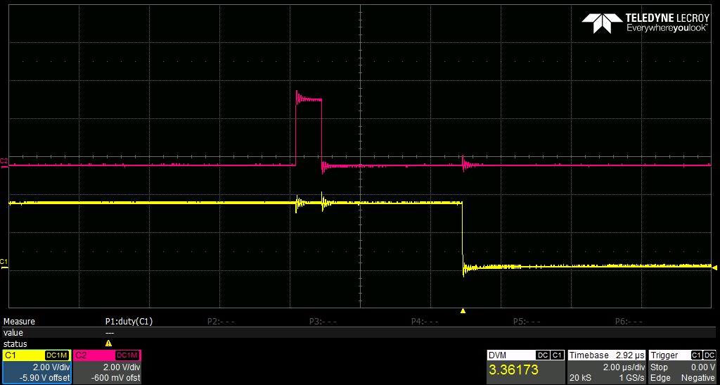
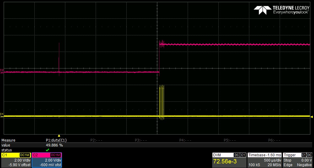
These are the settings I'm using for my registers. I am able to write all of these registers, and read them back. IDAC0 picks up the ID bit, so I know these are good values.

Second, I'm able to observe from the hardware, that the two 1mA current sources are working, since I have 1.64V across my REF0, and around 110mV across the RTD.

The RTD I'm using is 100 Ohms, ~110 at room temperature. I'm also getting 2.048V across Vref.

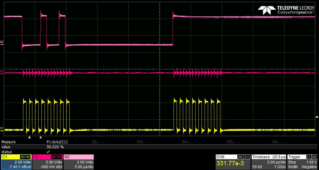
My process for  config is:

  • Set START Pin High
  • Send SDATAC
  • Wait for DRDY
  • Write first 15 registers
  • Wait 500us
  • Send SDATAC
  • Wait for DRDY
  • Read back first 15 registers 

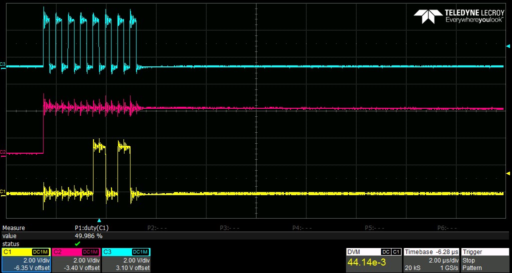
However I'm having issues when I try to read the data.

  • Verify that RST and START are still high (via printout)
  • Send SDATAC
  • Wait for DRDY
  • Assert CS Low
  • Send RDATA
  • Send xFF, receive first byte
  • Send xFF, receive second byte
  • Send xFF, receive third byte
  • Asset CS high

However all bytes that I receive are zeros. The all zero values are the same regardless of whether or not the RTD is plugged into the board or not.

I've also attempted to get data by pulsing the START pin and then using the SDATAC/RDATA method to read the bits in. The results are the same. I've also tried waiting a full second after SDATAC rather than waiting for DRDY.

Any advice? I'm pretty confident that it's a firmware issue, since the voltages on the pins are exactly what I'd expect them to be for this set-up. However, due to space constraints I don't have easy probing points for the data signals.

  • I had to scrape a via and solder a wire to it, so the signals aren't as clean as they would normally be.

    SCLK top, MOSI middle, MISO bottom.

    This is sending RDATA 0x13, followed by 0xFF. Nothing received on MISO.

    Zoomed in on the first RDATA transaction.

    ----------------------------------

    Successful SPI transaction during register reads

  • Hi Eric,

    Thanks for your post and welcome to the forum! 

    I know you said it's difficult to probe, but can you probe /CS to see if it's actually being driven low as an output by the MCU GPIO? With the resistor installed, it may be having a tough time actually being driven low. You may want to un-install R42 to verify that this isn't causing the issue. Additionally, I do not see the extra /RESET command after CS is being taken low. There are some timing delays that must be accounted for as well. 

    Take a look at 10.1.7 in the datasheet for an example.  

    http://www.ti.com/lit/ds/symlink/ads1246.pdf

  • Hi Alexander,

    Thank you for your reply. Since the ADS1247 is sitting on a dedicated SPI lane, I've tried permanently keeping the /CS signal low. This has produced identical results.

    I am able to write the registers, and read them back. 

    I've updated my config process:

    • Assert START High
    • Initialize SPI bus
    • Take CS low, and stay low
    • Send Reset Command
    • Wait 1 ms
    • Send SDATAC Command
    • Wait for DRDY falling edge
    • Wait 50us
    • Write 15 registers,
    • Readback and verify (this returns true)
    • Send SYNC command (I've also tried RDATAC here).

    Read Data

    • Wait for DRDY falling edge
    • Send RDATA Command
    • Read in 3 bytes, while keeping MOSI high via 0xFF / NOP command.
      • (I've also tried issuing SDATAC at the begining and then issuing SYNC or RDATAC at the end)

    The results are all the same. I can successfully read and write registers, but the ADC output code is always zero.  I've tried this on three different boards with identical results.

    Here is my code for the Config. This much I'm sure works.

    bool ADS1247Config(void)
    {
        usleep(16000);
        GPIO_init();
        GPIO_write(ADS1247_START, 1);
        SPI_init();  // Initialize the SPI driver
        SPI_Params_init(&rtdSpiParams);  // Initialize SPI parameters
        rtdSpiParams.frameFormat = SPI_POL0_PHA1;
        rtdSpiParams.bitRate = 1500000;
        rtdSpiTransaction.count = RTD_SPI_MSG_LENGTH; // 1 byte
        rtdSpiTransaction.txBuf = (void *) rtdTxBuffer;
        rtdSpiTransaction.rxBuf = (void *) rtdRxBuffer;
        rtdSpi = SPI_open(SPI_RTD, &rtdSpiParams);
        GPIO_write(ADS1247_SCS, 0);
        ADS1247SendByte(ADS1247_CMD_RESET);
        usleep(1000);
        usleep(600);
        ADS1247SendByte(ADS1247_CMD_SDATAC);
    	ADS1247WaitForDataReady(0);
    	usleep(50);
    	//write the desired default register settings for the first 4 registers NOTE: values shown are the POR values as per datasheet
    	ADS1247WriteRegister(ADS1247_0_MUX0, 15, regArray);
    	ADS1247ReadRegister(ADS1247_0_MUX0, 15, regArrayReadBack);
    	ADS1247SendByte(ADS1247_CMD_SYNC);
    	if((regArrayReadBack[0]) == regArray[0] && (regArrayReadBack[10] != regArray[10]))  /// checks that register 0 wrote okay, and that register 0x0A picked up the ID bit.
    	{
    	    return 1;
    	}
    	else
    	{
    	    return 0;
    	}
    }

    And here is my Read Data:

    long ADS1247ReadData(void)
    {
        long Data0;
        long Data1;
        long Data2;
        long Data;
        //ADS1247SendByte(ADS1247_CMD_SDATAC);      // 16 or 17
        while (!(GPIO_read(ADS1247_DRDY)));
        while (GPIO_read(ADS1247_DRDY));
        usleep(10);
    	// send the command byte
    	ADS1247SendByte(ADS1247_CMD_RDATA);        // 12, but I've also tried 13
    	// get the conversion result
    	Data0 = ADS1247ReceiveByte();
    	Data1 = ADS1247ReceiveByte();
    	Data2 = ADS1247ReceiveByte();
    	Data  = ((Data0 << 16) | (Data1 << 8) | Data2);
    	// sign extend data if the MSB is high (24 to 32 bit sign extension)
    	if (Data & 0x800000) { Data |= 0xff000000; }
    	//ADS1247SendByte(ADS1247_CMD_SYNC);
    	return Data;
    }

  • Hi Eric,

    Thank you for the additional information. 

    Can you provide additional scope shots of the read data communication as well? Please include CS as well as MISO, MOSI, and SCLK. 

  • Probing all four of those at the same time is incredibly difficult. Instead I've done multiple 2 or 3 wire probes to piece together how they all relate to each other.

    ----------------------------------------------------------------------------------------

    Sending Read Command:

    MOSI, top. MISO middle, SCLK bottom

    --------------------------------------------------------------------------------------

    I had to zoom out in order to see the CS

    All 24 SCKs top. /CS Bottom.

    ----------------------------------------------------------------------------------------

    Zoom in of 4 SCK bytes, and then CS being asserted high.

    ----------------------------------------------------------------------------------------

    /DRDY top, CS bottom.  CS is triggered after negative edge of DRDY

    ----------------------------------------------------------------------------------------

    /DRDY top, SCK bottom. After about 1.5ms, the 24 SCKs are issued. /DRDY goes high on first SCK.

    ----------------------------------------------------------------------------------------

    /DRDY top, /CS bottom. First DRDY pulse is hard to see, but it is slightly before CS goes low.

  • Additional update:

    If I alter the values of FSC I am able to force an output of 0xFF800000. So data read is working.

    However, if I leave FSC alone and only change OFC the output remains zero regardless of register values. I tried 0x000001 and 0xFFFFFF. All return zero.

    I measured the voltage across the input capacitors C53 and C54, and again they are what I would expect. 110mV, and 1.65V. These voltages also appear across the pins of the chip.

    DVDD and AVDD have almost no ripple what so ever, And both DGND and AGND share the same plane. Return plane is also very quite. 

    I'm getting identical results on all three of my boards.

    Here is snap of the layout. The three layers above the IC/traces are solid ground  and power planes.

    The only layout issues I can think of the trace running under the package, and pin 8 not having  a nearby ground via

  • ISSUE RESOLVED

    I was writing over the FSC register, which has a reset value of 0x400000. Since I'm writing every register sequentially from an array, updating this value to 400000 resolved the issue.

  • Hi Eric,

    Thank you for providing the additional scope shots. 

    I think the issue is related to writing the FSC0, FSC1, and FSC2 (full-scale calibration) registers. The automatic test equipment calibrates these gain registers, and they change for each PGA setting. Since they have been written to be 0, the conversion result is multiplied by 0, and therefor 0 is present on the output. The OFC and FSC registers should not be written to. Try just writing to the first 4 and last 5 registers and let me know how it goes. 

  • You're a full minute too late :D

    But this was indeed the issue. Thank you for looking into this.

  • Hi Eric,

    Very happy to hear that this resolved the issue! My pleasure, please let us know if you have additional questions or concerns by starting a new post.