

Part Number: ADS1247
Hi sir,
can you give me some suggestion on the GND layout and VDD circuit design method that maximize the ADC performance.
1) GND layout method
According to 12.1 (layout guidelines) of the data sheet, it is possible to separate the analog plane (AGND) and digital plane (DGND), but it is not required.
Please tell me more about this.
First, should AGND and DGND be separated for best performance?
(Is it the same performance without separation?)
If they are separated, is it correct to connect them under the ADC to eliminate the potential difference between AGND and DGND?
Is it better to place Amplifier and ADC (including digital signal pins) on the analog plane, place MCU and Interface on the digital plane, and separate them by Optional split as shown in Figure 123 and Figure 124?
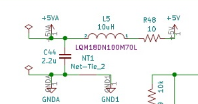
In my schematic, AGND and DGND of the ADC are separated.
2) VDD circuit design
To get the best ADC performance,
Which is better, one is to connect AVDD and DVDD to the same VDD plane, and the other is to separate AVDD and DVDD.
In my schematic, they are separated by an LC filter(L5,C44).
(Is it better to separate power supply by LDO?)
3)Application
If you have any application reports or information, please share them to me.
