


Hello,
We have a custom board with ADS54J66 and have observed crosstalk between ADC input channels C and D. Please find the schematic attached below - 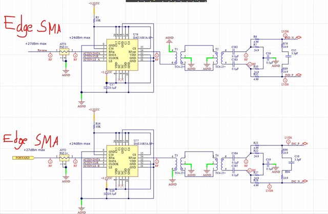
The transformer is https://www.minicircuits.com/pdfs/TC4-25+.pdf . SMA connectors are edge mount.
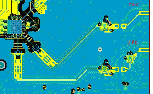
Please find the partial layout attached below -
The traces are 50Ohm single-ended coplanar waveguide on top layer. Trace width 15mil, ground spacing 6.8mil and dielectric thickness between top layer (layer 1) and ground reference layer (layer 2) is 10mil . The dielectric material is Rogers 4350B. The ground plane is single, solid and not split.
The layer stackup is -
TOP (Blue)
GND
POWER
GND
POWER
SIGNAL
GND
BOTTOM (Yellow)
Polygon pour on top and bottom layer.
Without polygon pour.
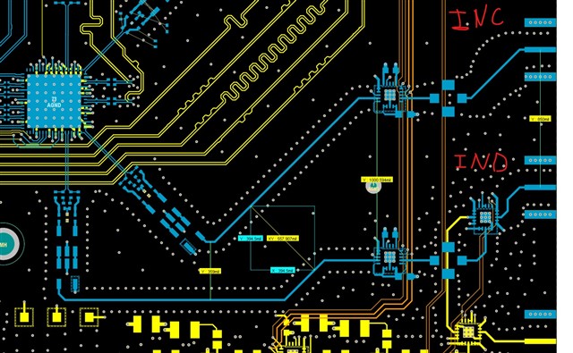
The shielding vias along C and D signal traces are at a distance > 5x the trace width.
The distance between the edge mount SMA connectors is 850mil and the distance between the signals when they run parallel to each other is around 600mil and 360mil as shown in the photo.
Is it recommended to rotate the C channel transformers and components such that they are perpendicular to D channel transformers and components ?
Is it recommended to add a keepout between C and D transformers polygon?
Could you please recommend any other ways to reduce crosstalk in the layout. Thank you.
