This thread has been locked.

If you have a related question, please click the "Ask a related question" button in the top right corner. The newly created question will be automatically linked to this question.

ADS1232: Sampling time error

Part Number: ADS1232

Hi,

Good day. I hope you are well.

Our customer has the following question regarding the ADS1232.

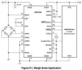
"I am user of ADS1232 analog to digital converter chip.

I set ADC sampling speed as 80Hz by provide HIGH voltage to SPEED pin as your datasheet described.

However, it is operated in 10SPS or 80SPS randomly, not 80SPS constantly.

Does ADS1232 chip have any other algorithm to convert sampling speed?"


Can you please assist us with this matter? Thank you for your support.


Regards,

Cedrick

  • Hi Cedrick,

    Can you provide a schematic?  The ADS1232 is a pin controlled device and all digital input pins must be at the appropriate level for operation and not floating.  This includes Clock, Gain, Address, and Temp pins. The PDWN pin must also be set high and not floating or operation will be unpredictable.

    If this appears and checks out correctly, then it would be helpful to see oscilloscope or logic analyzer shots of the DRDY/DOUT pin to observe the behavior.

    Best regards,

    Bob B

  • HI Bob,

    Good day. I've just received a response from our customer. Kindly see below.

    "Hi, I don't have schematic files sorry.
    I am using this commercial board of which pins are directly connected to ads1232 chip.

    I think the schematic is as same as your ADS123X datasheet's typical application schematic example as follows.


    But I directly connect SPEED pin to AVDD (5V) in order to employ  80SPS mode.
    Could it be possible to make the problem?
    I'm looking forward to your reply"

    Thank you for your help.

    Regards,

    Cedrick


  • Hi Cedrick,

    Using a breakout board is fine, but I have no idea how the customer is actually connecting up the device.  Showing a block diagram is not very helpful.

    For example:

    • How is the CLKIN pin connected or is a crystal being used? 
    • What are the actual voltages on A0 and TEMP pins? 
    • What are the actual voltages on the GAIN pins? 
    • What is the voltage on the PDWN pin? (If this pin is connected to a micro GPIO this voltage must be pulled high and cannot be in a float state.)
    • Are all of the supply pins including the ground pins connected correctly and verified?

    All of these pins could affect the output data rate.  Another problem with using a breakout board is performance.  It is extremely difficult to achieve the high levels of performance using a prototyping solution.

    Best regards,

    Bob B