1. As shown in Figure 1, the latency of TX_TRIG is between 0.5ns and 0.4*ts.Assuming an ADC clock frequency of 62.5M, this translates to a latency of between 0.5ns and 6.4ns.Obviously this is a very large time span, more than an order of magnitude.This can sometimes be troublesome for timing design.
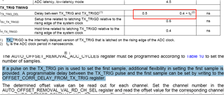
Continuing to review the specifications, you find that the delay between the TX_TRIG signal and the first sampling clock appears to be programmable, as shown in Figure 2.I don't know if my understanding is correct.If it is programmable, what is the correspondence between the 8bit OFFSET_CORR_DELAY_FROM_TX_TRIG register and the delay?This is not found in the specification.
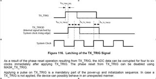
2. As shown in the figure below, when the system clock signal receives TX_TRIG signal twice in a row, 4-6 clock data will be destroyed immediately.Phase reset can be disabled with the MASK_TX_TRIG register.Do not know my understanding is right?
3. In addition to the timing constraints between the TX_TRIG signal and the system clock, what are the other constraints?
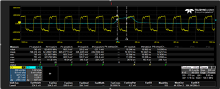
4. The following figure shows the timing relationship between TX_TRIG and system clock measured at the pin of AFE58JD28 of the board card. Does it meet the timing requirements?Does the timing still meet the requirements as the temperature changes and the differences between devices change?