This thread has been locked.

If you have a related question, please click the "Ask a related question" button in the top right corner. The newly created question will be automatically linked to this question.

PCM1794 frying

Other Parts Discussed in Thread: PCM1794, LM317, PCM1794A

Hi for all,

I have an intresting phenomenon with this DAC IC-s. I guess what the problem can be, but would like to have a confirmation.

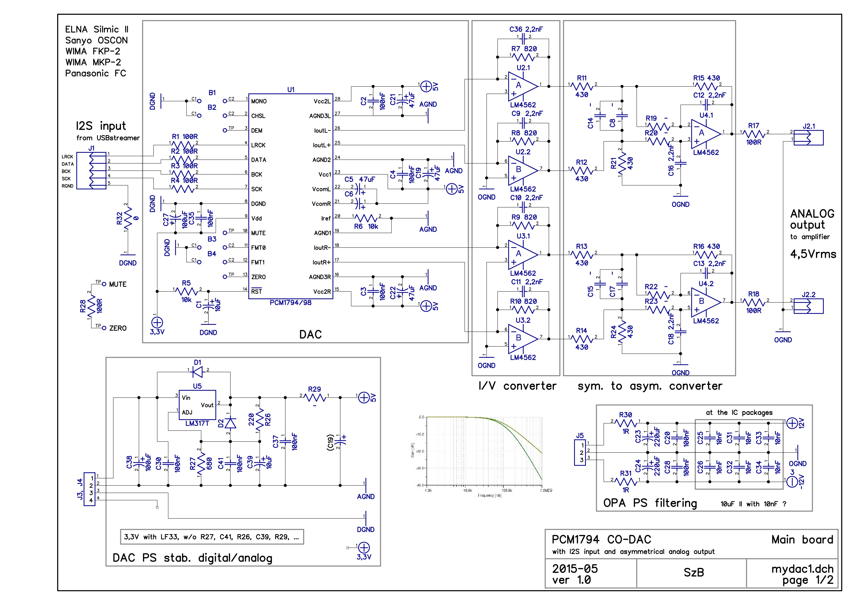
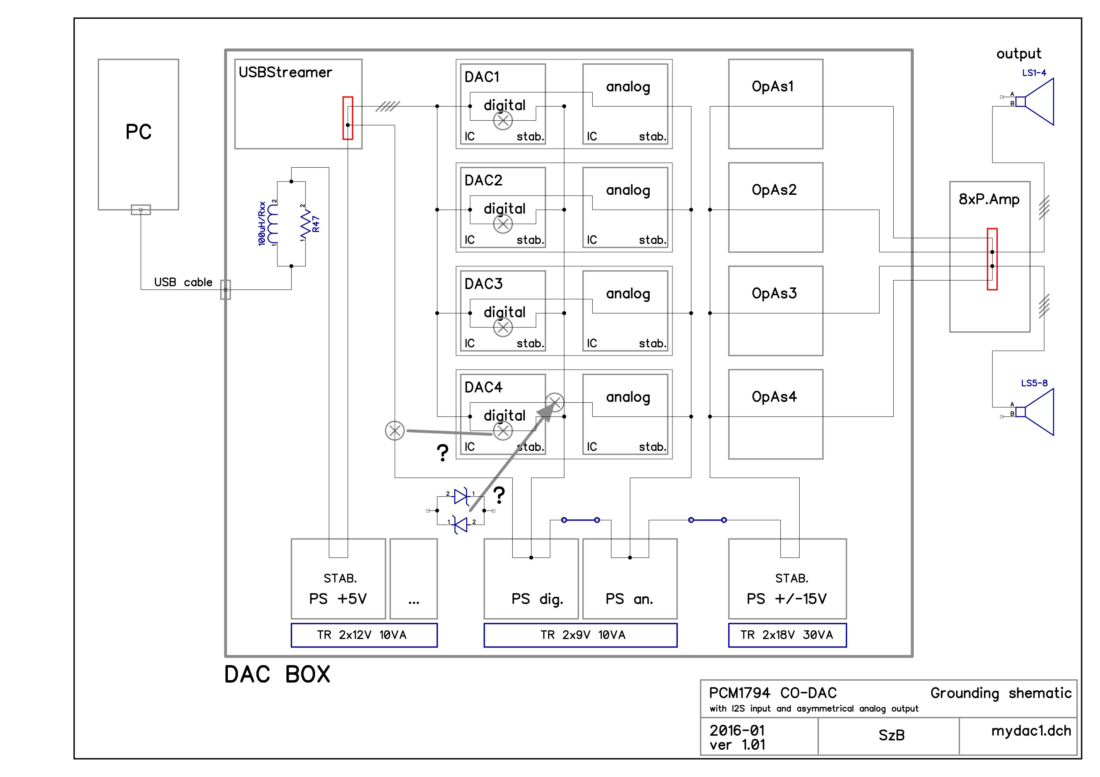
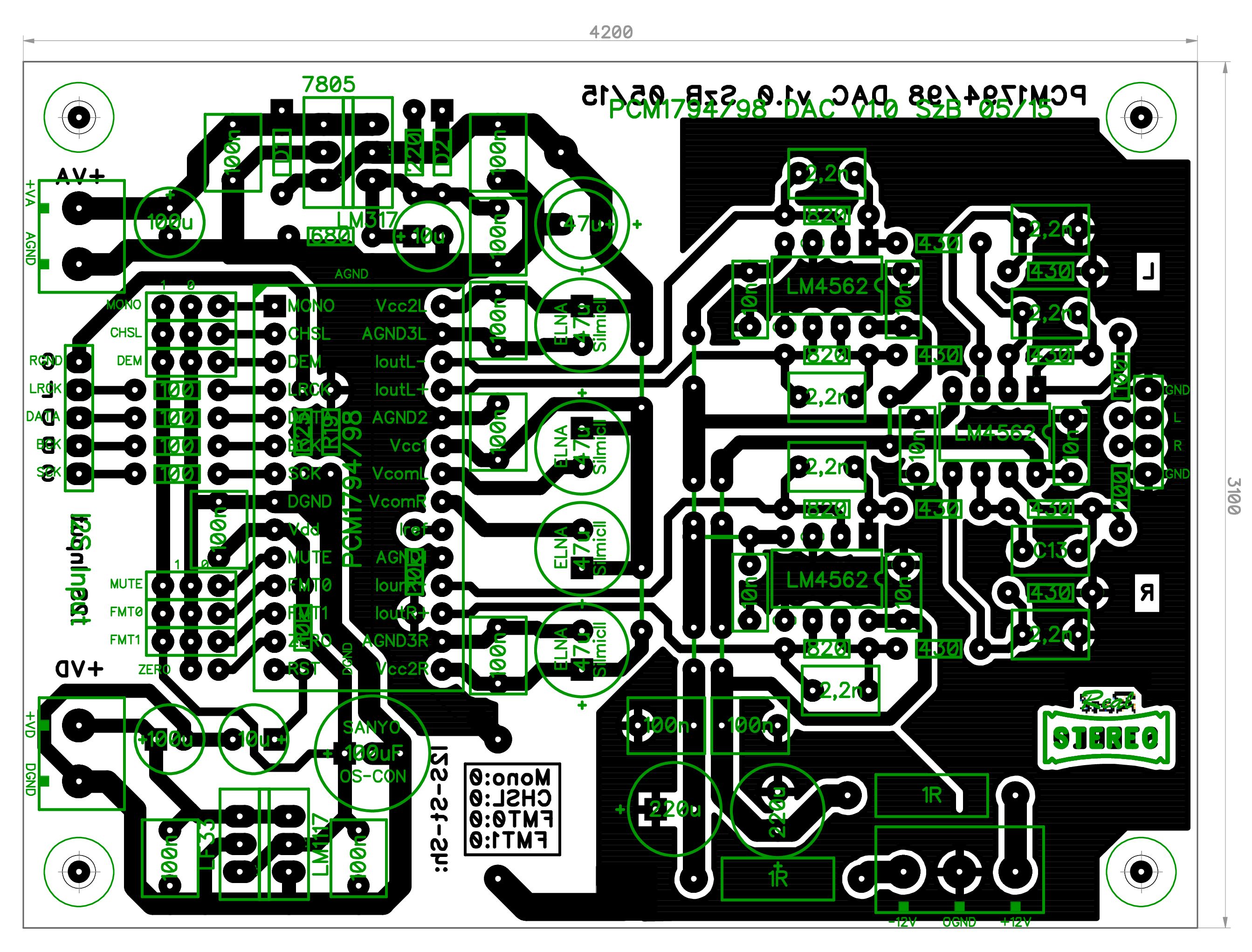
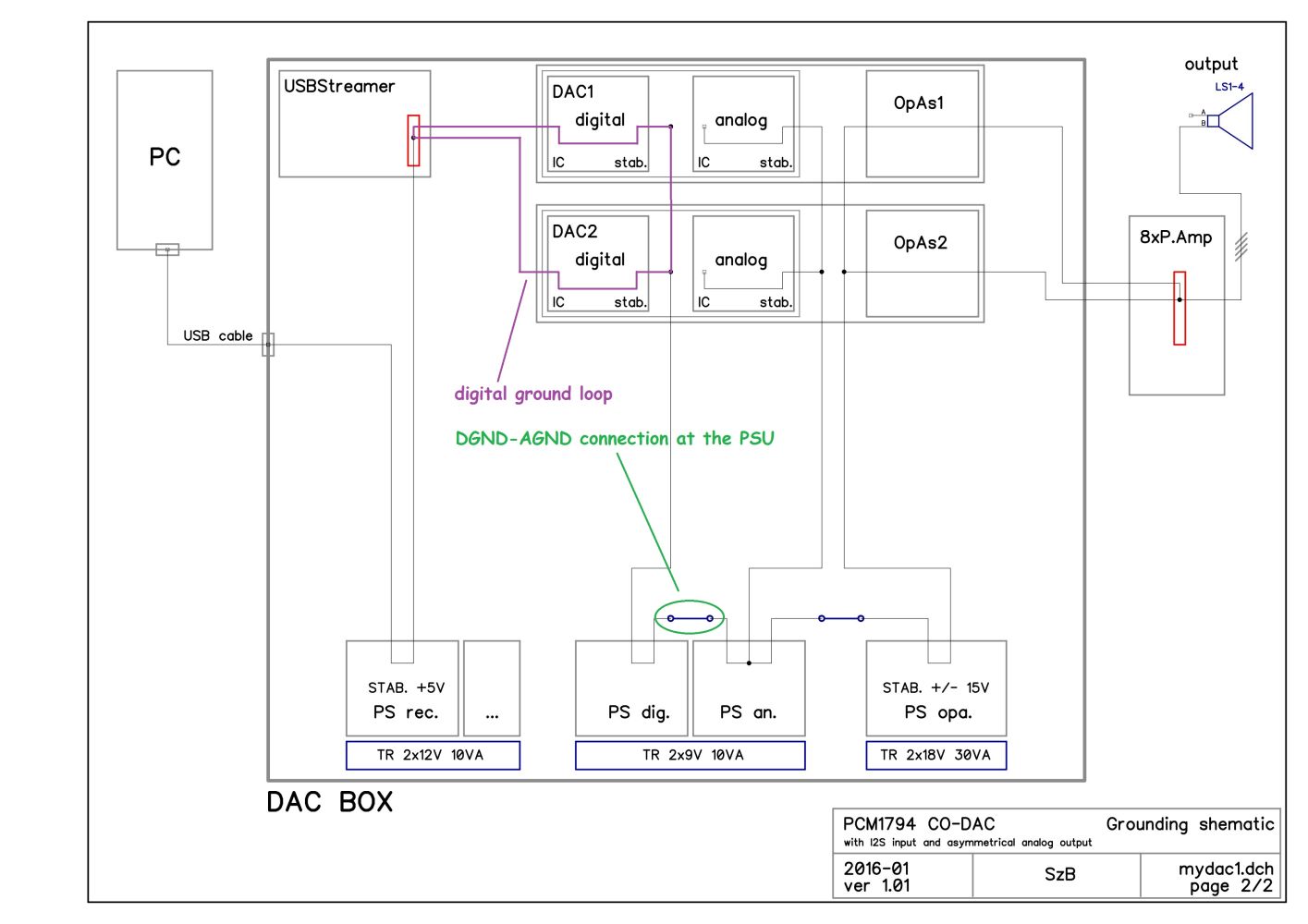
I have built a multichannel DAC with PCM1794. There are 4 separate (1 layer, through hole) panels with one IC pro panel in stereo mode with I2S inputs.

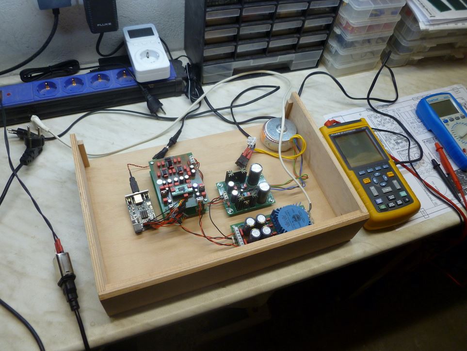
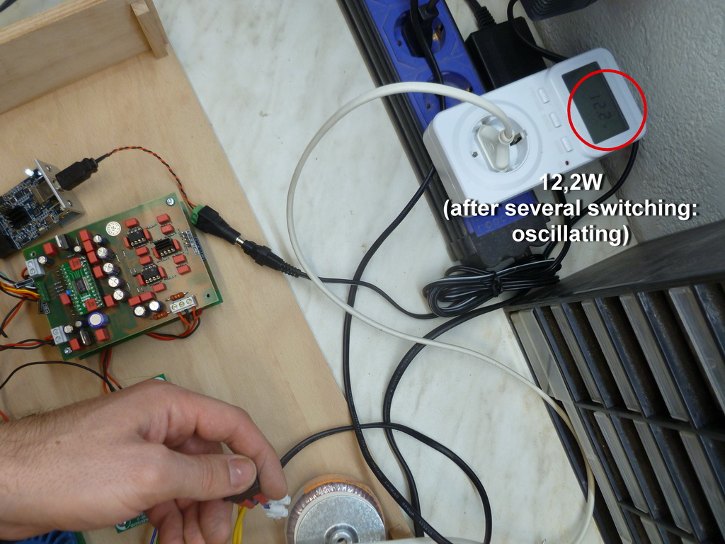
The receiver is the MiniDSP USBStreamer (I2S output). Please see attached picture (it is not my actual setup(!), only my first test arrangement with only one panel).

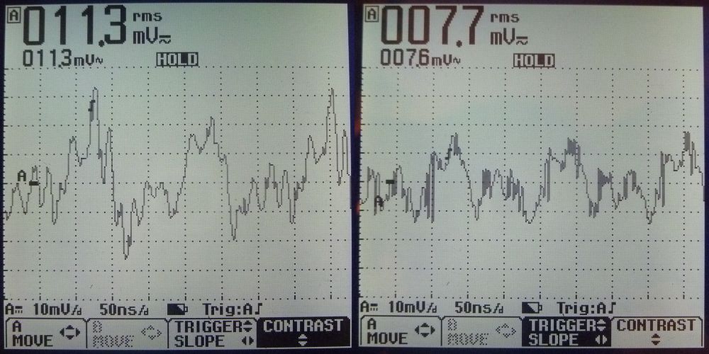
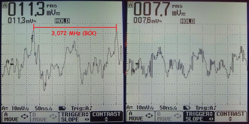
The problem comes when only rarely, as I turn on the system, or: I turn on-off only the PSU of the OPAs. In this case, the current consumption of the DAC on the 3,3V (digital) side is going to be the 5-10x of the normal, the IC is getting very warm, an there is no sound coming out...:( I turn of course immediately out, and next time everything normal....

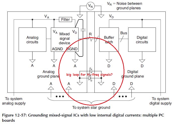
So my suspect: the problem can be that the digital and analog grounds are not connected directly by the DAC IC, but also at the PSU (see short connection). I have made it so because I have 4 panels and only one (double) PSU, and I wanted to avoid ground loops!

Is my insight correct? How shoud I arrange this setup to have a good and stable layout?

Thanks!!

(more pictures or shematics are of course by request available!)

  • Hi Cisga,

    i am not sure at the moment if the grounds are truly connected inside the part, I will have to look into that. At the moment I am wondering what your startup sequence looks like in terms of the analog and digital rails. The startup of the part is gated by the VDD voltage and SCK periods.

    As for layout recommendations, we recommend one single ground with good partitioning of the PCB so that return currents tend not to cross each other.

    Justin
  • Thanks Justin!
    I have posted some other pictures. I forget to say, this overhearing (oscillating?) occours ONLY, if the receiver (USBStreamer) is connected and powered!
    To make a 2 side PCB (with a full -or splitted- ground plane) is not so easy for me at home, so I try to clear first this setup...:)
  • To make it visually easier, made some photos from the case.... I have made some other power measurements too.

    The power consumptions of 2 (!) DAC panels (3,3 and 5V, without the OPAs) measured on the primer side, incl. PSU (10VA 2x9V transformator, double bridges with BYV27/150, LM317 for 5V, LF33CV for 3,3V):

    - normal operation without receiver: 1,1W

    - normal operation if receiver turned-on: 1,4W

    - operation if played music: 2,5W (the ICs are not hot but warm /ca. 40-50 C/!)

    - operation after played music: 2,3W (falls not down to 1,4W, ONLY if I turn off-on the receiver!!!)

    - oscillating (???) if unwanted transients are presented: 12,2W (the ICs are hot />50 C/, they would be fry I think)

  • Hi Csiga,

    Is it possible to get more information on what is happening with the inputs to the PCM1794A, such as the I2S input (SCK, BCK, LRCK and data) and the voltages on the supply pins? I have not run into a case of these parts acting this way, so I am not sure why this is happening. What does the speaker output during this state?

    Justin
  • Thanks Justin,

    With a cheap multimeter controlled the supply voltages stay stable.

    I have two pics now, but they are made in "normal" state (LRCK and SCK from the USBStreamer measured at the DAC inputs, after the R100 resistors, seems to be 48kHz mode).

    I'll try to do some measurements, but I have only a 20MHz Fluke 123 scope from my workplace (sometimes)....

  • I have made some other measuremens!

    My scope resolution is only 5mV, so I had the idea to measure at the loudspeaker terminals to have large enough signal levels.

    It is definitely interesting! It is NOT the resonanting state where the ICs are getting hot and not working, it is only the "normal" mode as I can listen to music.

    The outputs of my DAC panels have 2Vrms level, the signal amplifying of the power amp is 16x (24dB).

    Let's see the measurements. The first pictures are in the following cases, there are essentially not differences (I would say it is normal):

    - only my amps, without DAC box.

    - OR amps with the OPAs powered only.

    - OR amps with DACs and OPAs powered, when the receiver (USBStreamer) is NOT powered.

    - OR amps with DACs and OPAs and receiver powered, but ONLY 1 DAC panel active (and NOT 2 or more!)

    The secound pictures are in the following case:

    - amps with DACs and OPAs and receiver powered, all the 2 DAC panels active!

    As we can see, in this case there is a remarkable resonance at 250-400kHz. I can not hear it, but the loudspeakers are a little bit noisier. So, this is not normal...

    Is it created simply by ground loops in the digital area?

    I have measured the DGND - AGND voltage at the DAC pins in this two cases, because these are not directly connetcted at the IC, like I mentioned before.

    Left the "resonant" (2 panels), right the "normal" (1 panel) fall.

  • For a better understanding what am I talking about see my actual grounding shematic...

  • After a little analysis I clearly recognized the most dominant 3,072 MHz BCK signal coming from the USBStreamer

    between the DAC-IC DGND and AGND pins, but I think the others are there too...:(

    So my question is clear: can these voltages cause the 250-400kHz output noise???

  • I have found some information from AD: "Grounding Mixed-Signal Devices with Low Digital Currents in a Multicard System".

    But I am not sure it is a good idea....

    I think the I2S signal and grounding wires should be kept as close as possible together to avoid large loops that means large inductance for hi frequency signals.

    Or am I wrong??

  • No answer??? :(
  • Hi Csiga,

    We recommend one large ground plane for the entire PCB, with good partitioning on IC placement to keep return currents from different signals crossing paths. Having a noise on the output at 250 kHz to 400 kHz sounds like noise from a switching power supply. Are your power circuits using switchers that switch in that frequency range?

    Justin
  • Thanks Justin, I will do my next project with 2 layers and large ground planes, but now I have to make first this correctly (so or so)...:)
    I do not have any switching supplies, only linear regulators: DAC 5V: LM317; DAC 3,3V: LF33CV; USBStreamer 5V: LT1963.

    Like described before, this occours only, if all the 2 panels are connected, and the USBStreamer is switched ON!!
    I am afraid of some unwanted ground loops, but am not sure where this 250 kHz to 400 kHz resonance is coming from...

    The DAC IC can not produce this, even when the DGND and AGND pins are not directly connected at the IC package??
    If not, than is must be generated by the USBStreamer (but no idea what exactly) or for example a noise signal from outside (e.g. PC psu) catched up by the loops or some other parts...