This thread has been locked.

If you have a related question, please click the "Ask a related question" button in the top right corner. The newly created question will be automatically linked to this question.

DAC3482EVM: Phase noise out of DAC higher then DAC CLK Phase noise?

Part Number: DAC3482EVM
Other Parts Discussed in Thread: DAC3484, DAC3482

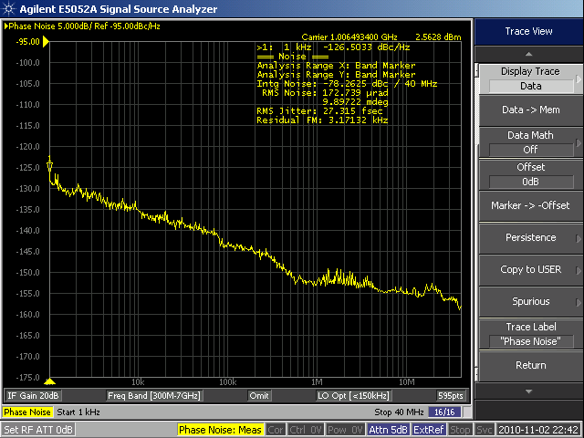
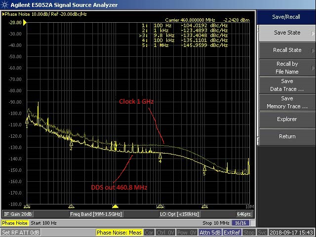
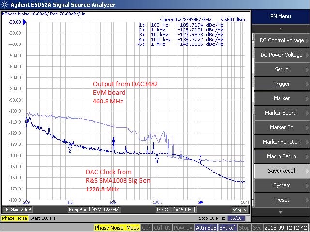
I am using the DAC 3482 as a DDS using the NCO in the part.  My clock frequency is 1228.8 MHz and I'm generating a signal at 3/8 of Fc (460.8 MHz).  

As can be seen from the picture below the phase out of the DAC is higher then that of the clock.  I would expect the DAC to be approximately 8dB lower or at the noise floor of the part which looks to be about  -145 dBc/Hz.  The results are the same when we input the clock from the LMX chip or bypass it and feed the clock to the DAC directly from the signal generator.

Any help you can provide would be welcome.

  • Hi Thomas,

    take a look at the following app note:

    it talks about the intrinsic phase noise of the DAC3484/82 family.

    Another way to improve the phase noise is to inject a really nice analog power supply (not the digital power supply) (or even the battery for clean source) to the VDDCLK1.2V. This is the clock buffer path for all the DAC sampling clock, so any noise on the power supply will modulate onto the output. If the power supply is clean, then the phase noise could be further improved. 

  • Kang,

    Thank you for your quick reply. I have already read the app note, it is very interesting and has a lot of good information but I don't think it answers my question. We had already tried using separate linear power supplies with no noticeable improvement but I will try using a battery.
    If you look at the picture the phase noise response out of the DAC3482 resembles that of a loop filter for a PLL. That is why we tried bypassing the LMK chip and disabled the PLL of the DAC3482. I can download the registers from the DAC and send them if that would be of use.

    Thanks again for your assistance.
    Tom
  • Thomas,

    I think the first step is for you to understanding the reason behind the step function for your measurement. Please lower the output frequency of the DAC, and also perform initialization of the NCOs to make sure the NCO accumulators are initialized correctly.

    You can try to duplicate the test results for phase noise through the following app note:

    You will need to refer section 3.4 of the following app note to initialize the NCO correctly:

    In the past, the E5052 have problems distinguishing the two Nqyuist zone tones from the DAC. You generated the 460.8MHz tone, but there is actually another tone reflecting around 614.4MHz at 768MHz. You may need to add a filter to allow the E5052 to better resolve the Nyquist image.

    attached are two measurements done a long time ago with a Wenzel 1GHz oscillator with the DAC output at around 400MHz. You can see the DAC itself can achieve much better noise floor.

    DAC output at 402.59MHz

    Wenzel oscillator source at 1GHz

    Is this done on your own PCB or the TI EVM? Please try this also on TI EVM to duplicate the setup.

  • Kang,

    Again thank you for the quick reply.  The app note you sent are very interesting and may be useful as we move farther in the design but they do not answer my question.

    We are doing all our measurements using the TI EVM.

    We are not using the PLL internal to the DAC3482.  I have verified that bit 10 of register 0x18 is set to 0 so the PLL should be bypassed.

    We are not using the clock distribution chip (CDC62005) we are inputting the clock directly to the DAC on J22.

    We have tried many different combinations of clock and output frequencies all of which still have the pedestal response in the phase noise below 200 kHz offset on the output signal.  The level of the phase noise changes with the ratio of the output frequency to the clock frequency as you would expect but I don't understand how the output phase noise is higher then the input.  The noise out should be lower then the noise in in proportion to the divide ratio as long as you are above the noise floor of the DAC.

    The picture below shows the input clock (1 GHz) and the output signal at 460.8 MHz from an Analog Devices DDS chip AD9912.

    The output phase noise should be 20 LOG Fs/Fc.  20 LOG 460.8/1000 = -6.73 dB.

    As you can see the output noise follows the shape of the input and is very close to the theoretical value.

    Am I wrong to expect a similar result using the NCO in the DAC3482?

  • Hi Thomas,

    I expect to observe the same trend. Based on all the previous testing, this is the case.

    I do not expect the step response like you have in your data for the DAC3482. This is the reason I have asked have you made sure the NCO is initialized correctly in the phase/frequency counter to ensure the sine/cosine is generated properly.
  • Hi Thomas,

    Please update if the the NCO synchronization fixed the phase noise issue.

    If not, please provide snap shots of your GUI so we can review it here.

    I have two more thoughts about this regarding the tone generation:
    You will need to have the TSW1400 as your tone generation on the baseband. If the tone generation is not done properly, then you may encounter such issue.
    The DAC3484 family technically have a constant DC test input to bypass the LVDS bus. (this is the SIFDAC_ENA bit in 0x2D register and the SIFDAC value in 0x30 register). However, you will still need to make sure the LVDS DATACLK is toggled at least sufficiently to latch into the FIFO properly.

    -Kang