This thread has been locked.

If you have a related question, please click the "Ask a related question" button in the top right corner. The newly created question will be automatically linked to this question.

ADS1118 interfacing to pic30f by using SPI

Other Parts Discussed in Thread: ADS1118

Hi i am using pic30f5011 (16 bit ) controller and mplabc30 compiler,to observe the output of the program i am using terminal programming....

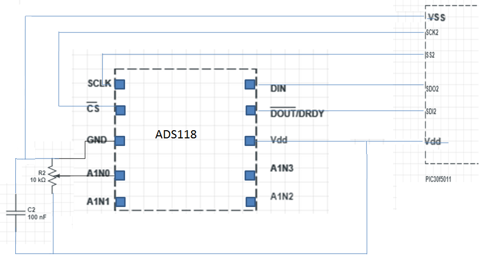
My task is to read Voltage readings by using ADS1118, i am new to SPI and And ADS1118...

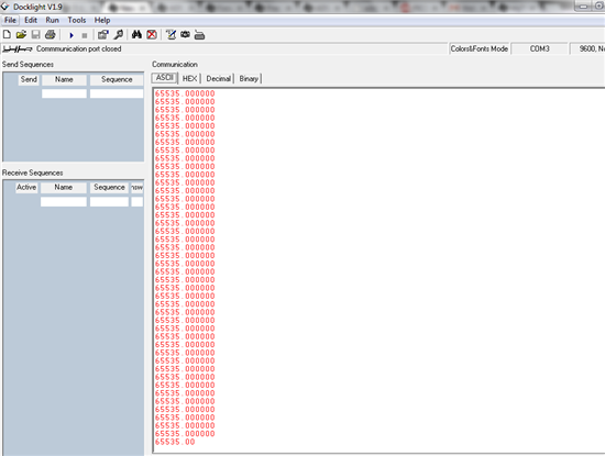
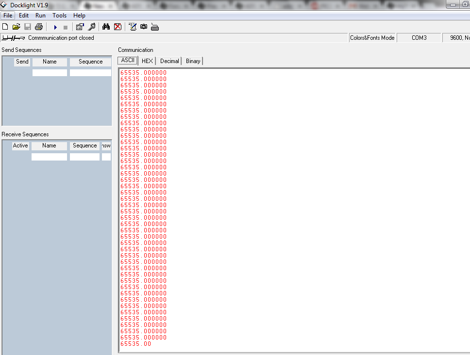
while running my code no errors... its showing output as 65536.. !

#define SCLK LATGbits.LATG6 //clock line
#define SDI LATGbits.LATG7  //SPI data input
#define SDO LATGbits.LATG8  // SPI data output
#define CS LATGbits.LATG9   // chip select


/// main starts here

int main()
{
        double temp,result; // variable to store output

	ADPCFG = 0; //ALL PINS in ANALOG form

	TRISGbits.TRISG6 = 0;   // SCK is an output
	TRISGbits.TRISG7 = 1;   // SDI is an input
	TRISGbits.TRISG8 = 0;  	// SDO is an output
	TRISGbits.TRISG9 = 0;   // CHIP SELECT AS O/P

        CS =1;
	uart_init();	//Uart Initialization
	SPI2_Init();	//SPI Initialization

	while (1)
	{
		CS =0;
		WriteSPI2(0x04EB);       // Configure ADS1118
		result = ReadSPI2(0x0000); // reading results from ADS1118
		CS =1;

		printf("%f\n",result);  

		Delay();
		Delay();

	}


}


/// SPI initialization
void SPI2_Init(void)
{


	SPI2STATbits.SPIEN 	  = 0;	//initially disable pin
	SPI2STATbits.SPISIDL  = 0;	//opertion mode idle
	SPI2STATbits.SPIROV   = 0;	// Rx overflow flag
	SPI2STATbits.SPITBF	  = 0;	//Tx buf full status
	SPI2STATbits.SPIRBF	  = 0;	//Rx buf full status
	
	SPI2CONbits.FRMEN 	  = 0;	//Framing support diabled
	SPI2CONbits.SPIFSD	  = 0;	//Frame Sync Pulse Direction Control on SSx pin bit 0-master,1-slave
	SPI2CONbits.DISSDO	  = 0;	//Disable SDOx pin bit,0=pin conreolled by module,1=Pin is controlled by associated port register
	SPI2CONbits.MODE16	  = 1; 	//Communication is word-wide (16 bits),0=Communication is word-wide (8 bits)
	SPI2CONbits.SMP		  = 0;	//SPI Data Input Sample Phase bit Master mode:0,1  Slave mode =0;      
	SPI2CONbits.CKE		  = 0;	//
	SPI2CONbits.SSEN	  = 1; 	//Slave Select Enable (Slave mode) bit
	SPI2CONbits.CKP		  = 0;  //Clock Polarity Select bit
	SPI2CONbits.MSTEN	  = 1;  //Master mode enabled
	SPI2CONbits.SPRE	  = 7;	//Primary prescalr 1:1
	SPI2CONbits.PPRE	  = 3; 	//Secondary Prescalar 1:1
	
//	IFS1bits.SPI2IF = 	0;  // Clear IF bit 
//	IPC6bits.SPI2IP	=	6;  // Assign interrupt priority
//	IEC1bits.SPI2IE	=	1; 	// Interrupt En 

	SPI2STATbits.SPIEN 	  = 1;
	printf("SPI2 init done\n");
}


void WriteSPI2(unsigned int data_out)
{   

   if (SPI2CONbits.MODE16)           // word write 
        SPI2BUF = data_out;
    else 
        SPI2BUF = data_out & 0xff;	  //  byte write 

}
unsigned int ReadSPI2()
{         
    /* Check for Receive buffer full status bit of status register*/
    if (SPI2STATbits.SPIRBF)
    {
        SPI2STATbits.SPIROV = 0;
                
        if (SPI2CONbits.MODE16)
            return ( SPI2BUF );        /* return word read */
        else
            return (SPI2BUF & 0xff);   /* return byte read */
    }
	return -1;                         /* RBF bit is not set return error*/
}


void Delay ( void )
{
    int temp;
    for( temp = 0; temp < 255; temp++ );
}

am i missing something in SPI or ADS1118? plz help me anyone

showing output like this :

 
  • My hardware connections are like this

    ADS1118 vs  Microcontroller connection is like this

    SCLK--------->SCLK
    CS ----------->CS
    SDO---------->SDI
    SDI----------->SDO


    4 Pullup resistors(4.7k) connected to SDO,SDI,SCLK,CS
    And Variable pot(10k) is connected to ADS1118 analog channel AIN0 (ADS1118 -4th pin) to vary the in put voltage to ADS1118

  • Hi Naga,


    It's a bit hard to read through code to debug a problem like this. I would take an oscilloscope shot of the communication and post it back to the forum.

    Recently there was a post about this device that might be applicable to your problem. I've written down the most important sections below.

    It's possible that the device is being given an invalid configuration. In this case, the ADS1118 is powered down and never converts. To write the configuration you must have bits 2:1 as ‘01’ otherwise the configuration will be ignored. It is outlined in the Conversion Register section on pages 21 and 22.

    For comunications, it's also best to issue a four byte transaction so that you can read back the configuration with bytes 3 and 4.

    In case you want to read it the original post is here:

    http://e2e.ti.com/support/data_converters/precision_data_converters/f/73/t/372229.aspx


    Joseph Wu

  • Hi Joseph Wu thanq for your reply, 

    currently  oscilloscope not available ...


    #include"SPI_2.h"
    #include"uart.h"
    
    volatile double temp,result;
    
    
    int main()
    {
    ADPCFG = 1; //ALL PINS in ANALOG form
    TRISGbits.TRISG6 = 0; // SCK is an output
    TRISGbits.TRISG7 = 1; // SDI is an input
    TRISGbits.TRISG8 = 0; // SDO is an output
    TRISGbits.TRISG9 = 0; // CHIP SELECT AS O/P
    CS =1;
    uart_init(); //Uart Init
    SPI2_Init(); //SPI INIT
    while (1)
    {
    CS =0;
     
    //Programmable gain amplifier configuration (011) ==> FS is ±1.024 V
    //Data rate (111) = 860 Samples Per Second
    //Data rate (000) = 8 SPS
     
    WriteSPI2(0x0000);
    WriteSPI2(0x060B); //06EB working with 0.2 volts difference
     
    Delay();
    Delay();
     
    result = ReadSPI2();
    temp = ReadSPI2();
    CS =1;
    
    Delay();
    Delay();
     
    printf("V %.5f\n",(double)result);
    }
     
    }
    
    } 


    Above modifications in my code ADC along with SPI working with some issues
     
    Issue 1 :The output voltage readings i am getting is 0.2 volts to 0.4 volts difference with actual ADS1118 input voltage
     
    Issue 2: Input voltage to the ADS1118 is maximum 5 volts and Minimum 0 volts (Variable),
     
    When i am increasing ADC input voltage from 0 to 5 volts at 2.5 volts ADC working fine beyond that voltage levels OUTPUT showing 2.5 volts only (No increment happening)..
     
    When i am decreasing from 5 to 0 volts at 0 volts showing results as 4.9 volts or 5 volts or may some times decreasing...
    where i am missing??How can i get exact resolution ??

  • Hi Naga,

    Joseph is out of the office this week. I try to help out for now.

    The most important thing when you want to measure a signal that swings between 0V and 5V is to set the FS to +/-6.144V (PGA[2:0] = 000).
    Please remember that you will only be able to measure signals up to 5V when using a 5V supply - and not up to 6.144 volts. That means you will not be able to use all available codes.

    In contrast to an I2C interface, pull-up resistors are not required on an SPI interface. They will only cause additional power consumption when a signal drives low.

    The SPI interface needs to be configured correctly. The interface of ADS1118  operates in SPI mode 1
    where CPOL = 0 and CPHA = 1.

    Regards,

  • Hi Joachim Wurker,

    thank you so much for your valuable reply now my code is working fine

    include headers
    #define OPV (6.144*2) //Peak to peak FS
    #define bit16 (65536U)    //2^16 
    #define MF 	(OPV / bit16)


    int main()
    {
    	ADPCFG = 1; //ALL PINS in ANALOG form
    
    	TRISGbits.TRISG6 = 0;   // SCK is an output
    	TRISGbits.TRISG7 = 1;   // SDI is an input
    	TRISGbits.TRISG8 = 0;  	// SDO is an output
    	TRISGbits.TRISG9 = 0;   // CHIP SELECT AS O/P
    
    	CS =1;
    
    	uart_init();	//Uart Init
    	SPI2_Init();	//SPI INIT
    
    	while (1)
    	{
    		CS =0;
    		WriteSPI2(0x0000);
    		WriteSPI2(0x80EB);     //04EB working
    	
    		Delay();
    		Delay();
    		Delay();
    
    		result = ReadSPI2();
    		temp = ReadSPI2();
    		CS =1;
    
    
    		Delay();
    		Delay();
    		Delay();
    		Delay();
    
    
    		digi_result= (result * MF));
    		result =0;
    
    		printf("V %.3f\n",(float)digi_result);
    		digi_result=0;
    		}	


    	}
    
    
    }

    I am using 5.094(max) volts input so i used FS +/-6.144 V,clock polarity set to 0,clock phase set to 1(trailing edge sampling) 

    i am getting the output with 60 or 50 milli Volts difference...
    but for 16 bit resolution we need to get accuracy in Micro volts...
    according to hardware there is no ripples(noise) in input voltage. is there any chances to increase accuracy??


    4 Pullup resistors(4.7k) are connected to SDO,SDI,SCLK,CS

    And Variable pot(10k) is connected to ADS1118 analog channel AIN0 (ADS1118 -4th pin) to vary the in put voltage to ADS1118


    increasing output voltage max 5 volts is working fine

    when i am decreasing above 0.4 volts reading voltage is fine but below 0.4 volts output is showing 5 volts(starting from maximum voltage), 4volts, 2 volts etc,...

  • Hi Naga,

    I am happy to hear you got the ADS1118 working properly now.
    However I will have to disappoint you. You will not be able to resolve uV of signal with the ADS1118. Maybe 100's of uV in your case.
    The smallest signal you can resolve with an ADC is limited by the LSB size. The LSB size of an ADC can usually be calculated as:
    1 LSB = FSR / 2n

    In the case of the ADS1118 the FSR = 2*6.144V so the LSB size equates to LSB = 2*6.144V/216 = 0.1875mV (as you implemented correctly in your code).
    You can not resolve signals smaller than that with ADS1118 when you want to measure a 0V to 5V signal.

    Could you explain to me in more detail what you mean by the following comments:
    "i am getting the output with 60 or 50 milli Volts difference" and
    "when i am decreasing above 0.4 volts reading voltage is fine but below 0.4 volts output is showing 5 volts(starting from maximum voltage), 4volts, 2 volts etc"

    How did you connect the negative input of the ADC to the pot?

    As the ADS1118 has some offset, you could potentially get a negative output signal when your input signal is close to 0V. Therefore you should make sure in your code to convert the twos complement correctly.

    Depending on what kind of pot you use, you might not be able to get as fine steps as you think you would.
    Could you hook up a precision voltage source to the ADC inputs instead and increase the voltage by 0.1mVs to see if the codes flip as expected? Maybe start with a slower sampling rate of the ADS1118 first.

    Regards,

  • thank you for your support Joachim Wurker,

    "i am getting the output with 60 or 50 milli Volts difference" and 
    "when i am decreasing above 0.4 volts reading voltage is fine but below 0.4 volts output is showing 5 volts(starting from maximum voltage), 4volts, 2 volts etc"

    i mean to say output voltage having linear error like these 2 cases..

    CASE 1: With 4.7k pullups on SDO SDI CS and SCLK

    INUPUT              Vs        OUTPUT 

    0.000 V(Min)       ==> 12.016 V  (difference is 12.016V)
    0.856 V                ==> 0.305 V (difference is 551 V )
    2.061 V                ==> 1.904 V (diff is 0.157 V)
    2.547 V                ==> 2.433 V (diff is 0.114 V)
    3.163 V                ==> 3.088 V (diff is 0.075 V)
    4.530 V                ==> 4.489 V (diff is 0.041 V)
    5.094 V(Max)       ==> 5.067 V (diff is 0.027 V)


    CASE 2: Removed pullups on SDO SDI CS and SCLK

    INUPUT              Vs        OUTPUT 

    0.000V(Min)         ==> 11.913 V  (difference is 11.913V)

    0.344V                  ==> 12.099 V  (difference is 11.755V)

    0.911V                  ==> 0.314  V  (difference is 0.597V)

    1.342V                  ==> 0.788 V  (difference is 0.554V)

    2.389V                  ==> 1.956 V  (difference is 0.433V)

    3.134V                  ==> 2.734 V  (difference is 0.400V)

    4.379V                  ==> 4.057 V  (difference is 0.322V)

    5.096V (Max)        ==> 4.808 V  (difference is 0.288V)

    I am using variable 10k pot  (Variable from 0 to 5V),  

    pot negative voltage directly connected to ADS1118 Ground 

  • Hi Naga,

    I am currently not 100% sure where those large errors could be coming from. Looks like some inverse gain error to me. I need to think about that some more. Would you be able to route the negative analog input (I think AIN1 in your case) directly to the other end of the pot, that way any disturbance coming from the GND plane would be removed.

    The pull-ups on the digital lines should actually not have any impact on the reading unless something in your layout is not optimized. As I said above, I would recommend leaving the pull-ups away. You could leave the one on /CS maybe.

    The large error at 0V input is definitely due to the fact, that you don't convert the twos complement properly. So you should get this corrected in your code.

    Regards,

  • Hi Naga,

    As we see that the condition appears to worsen with the removal of the pull-ups, I suspect that there may be some issue related to the communication.  First of all make sure that the SCLK is lower than the maximum of 4MHz.  I would suggest using an SCLK around 2MHz.  Faster clocks often produces higher noise.  Also, you might want to add some series resistance in the digital signal lines instead of using the pull-ups.  This will slow the edges of the fast rise time edges which in turn will also reduce overall noise.

    I noticed that in your code you are using delays.  You really have no way of knowing when the conversion is complete and when the results are current.  Normally what is done is using an interrupt driven system or a polling of the DOUT/DRDY pin to determine when the conversion completes.  Your configuration is using the start of conversion bit 15, but is configured for continuous conversions.  This may also be adding noise to the measurement, as the continual unnecessary communication to the ADS1118 may be adding noise.  If you are using continuous conversion mode, you only need to read from the device when the conversion completes.  You do not need to continuously write the same configuration.  If you use the single shot mode, then you can read from the device in the first two bytes and then send the start configuration for the next conversion cycle.  So you can use one or the other, but I suggest not using a combination of the two.  Adding the START of conversion to continuous mode has no effect.

    The last thing I would like to point out is that the difference in the measurement increases with the increase in the wiper of the pot with respect to resistance.  Generally I would not use a pot for this type of measurement as you change the sensor's (or pot's) output impedance with every adjustment.  In other words you are not able to consistently keep the impedance the same for each measurement.  The ADS1118 uses a switched cap input stage sampling the input at about 250kHz.  The charging of the input caps that are sampled will draw some current, and essentially creates a current divider with the pot.  I would use a true voltage source with low output impedance.

    One other point I should make is that you should account for both gain error and offset error of the system.  If you see a linear change across the measurement range and/or if you see a consistent shift in the values you can adjust your returned value to correct for these errors.

    We have seen your code, but not your schematic.  There may be some additional items that we are overlooking.  If you could send us the schematic it would be helpful.

    Best regards,

    Bob B

  • Hi thanks for your support again

    Without hardware changes (without Pullups), 2's compliment and interrupt based conversion modifications in my code now working fine but

    at lower data rate (8 samples per second) without pullups in my hardware getting output with constant difference like

    INPUT vs Output
    0.000 ==> 0.000V
    0.578 ==> 0.000V //Difference is (0.578)
    0.587 ==> 0.009V //Difference is(0.578)
    0.184 ==> 0.768V //Difference is(0.584)
    0.623 ==> 0.042V //Difference is(0.581)
    1.349 ==> 0.766V //Difference is(0.583)
    2.538 ==> 1.962V //Difference is(0.576)
    3.907 ==> 3.331V //Difference is(0.576)
    5.096 ==> 4.521V //Difference is(0.575)

    At higher data rate (860 samples per sec) output voltage is drastically fluctuating
    example 1:
    Input voltage 2.578 ==> Output Voltage will be fluctuating like
    1.953 V
    2.068 V
    2.047 V
    2.031 V

    Example 2: Input voltage 3.450
    Output voltage will be
    3.046V
    2.746V
    3.046V
    2.737V
    3.043V

  • schematic for my code

  • Hi Naga,

    I see we are making a little progress, but those results are not satisfactory yet.

    What is your register setting of bits MUX[2:0] in that case? It was '000' before as far as I saw.
    It should be '100' in this case.

    As I mentioned before it might be better to use input AIN1 as the negative input and connect the terminal of the pot that is currently connected to GND to AIN1.

    Regards,

  • thank you so much for your support Joachim Wurker ,Joseph Wu and Bob Benjamin


    My code is absolutely working fine now with tens of Micro Volts (below 0.5 Milli Volt) variation ...


    Some changes done in my hardware:

    1) ADS1118 A1N1 is connected ground so the disturbance coming from the GND plane would be removed.

    2) Added 2 series resistance(1k each) in the digital signal lines instead of using the pull-ups

    Some changes done in my Software:

    1) Instead of using delay  polling of the DOUT/DRDY 

    2) 2's compliment conversion

  • Hi Naga,

    that is great. Thanks for the feedback.
    Only one thing, 1k series resistors on the digital signal lines might be a little large. We usually recommend values in the 50-100Ohm range.

    Regards,