This thread has been locked.

If you have a related question, please click the "Ask a related question" button in the top right corner. The newly created question will be automatically linked to this question.

ADS130E08 Initial Flowchart and Captured Data Verification

Other Parts Discussed in Thread: ADS130E08

Hi,

I wrote the code as specified in the ADS130E08 datasheet flowchart (pg45).

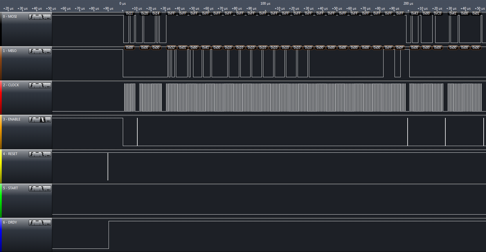
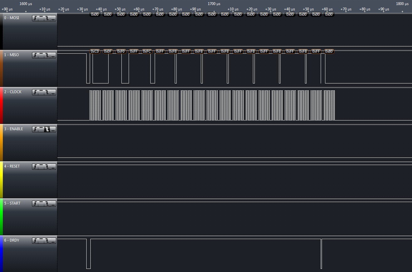
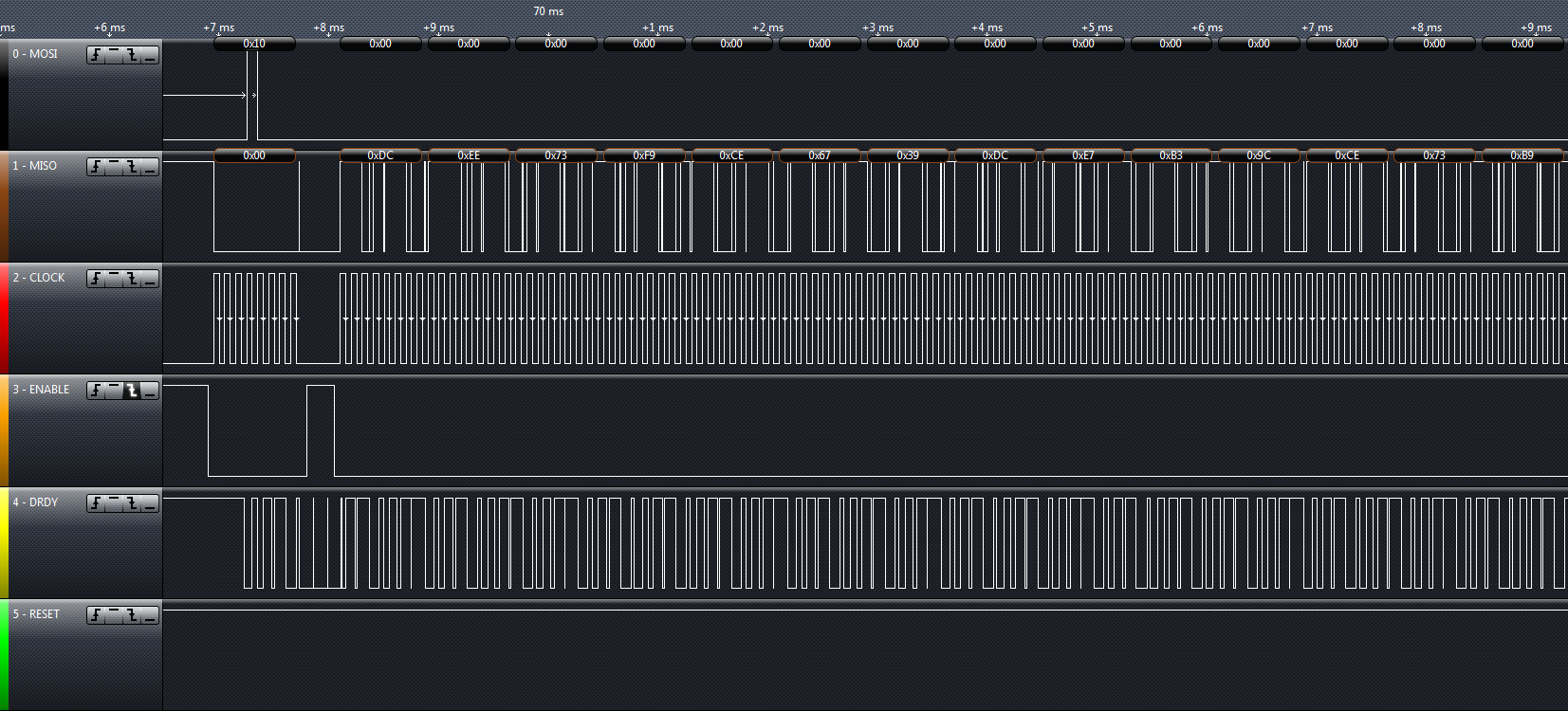
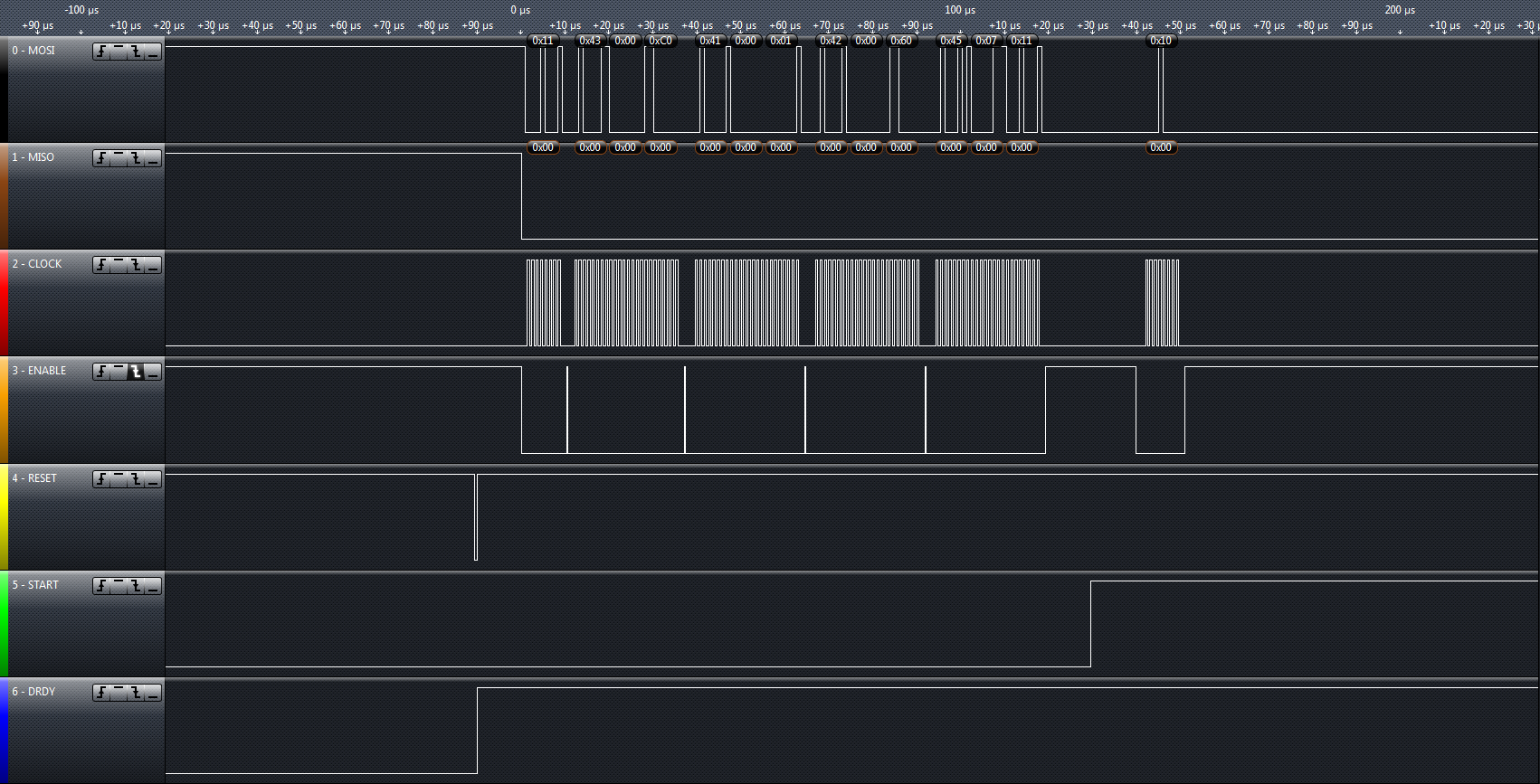
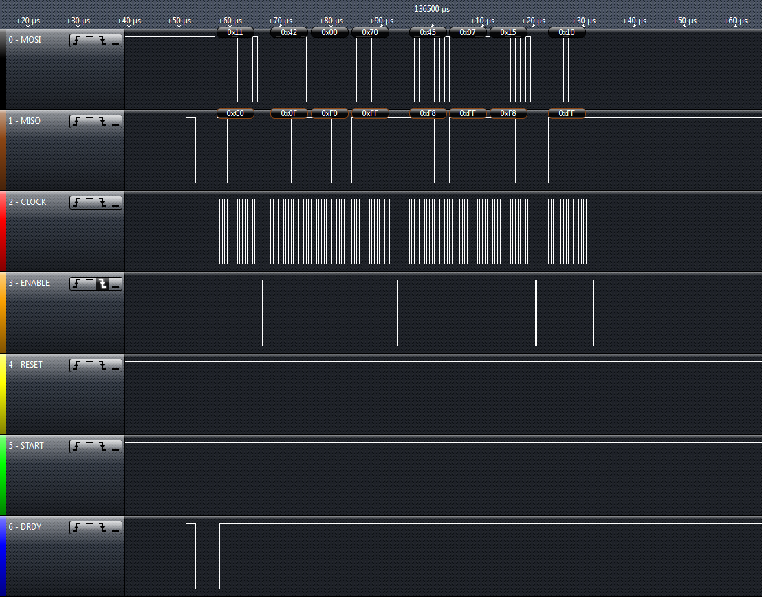
I've attached some logic analyzer pictures and I'd like some validation as to whether it is working correctly.

Logic Analyzer pictures based on Initial Flowchart:

1)      Reset Pulse -> SDATAC -> WREG config and set channel short -> START -> RDATAC

2)      SDATAC -> WREG config square wave test signal -> RDATAC

3)      Capture Data and output on terminal

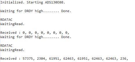
The last picture is my captured signal on the terminal. Received : 57375, 2304, 61951, 62463, 61951, 62463, 62463, 236

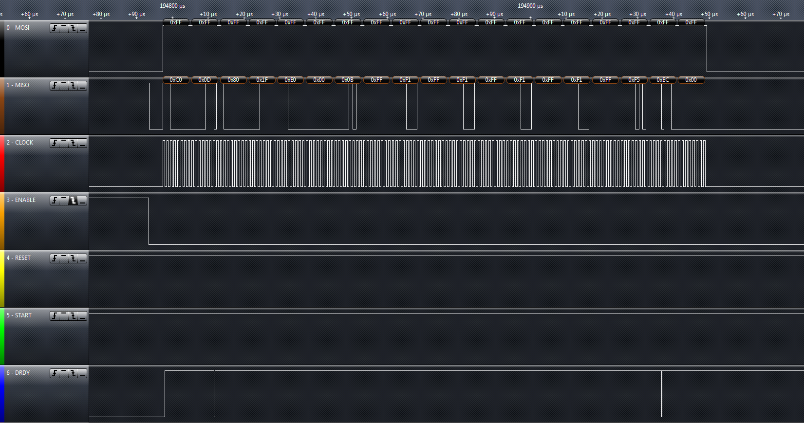
Is the received value correct? Anything to improve on (timing, etc)?

Thanks,

Stephen

  • UPDATE

    There are some important inconsistencies when I do RREG Read from Register.

    I power up the board, pulse RESET, and then send SDATAC Command as per flowchart.

    Then I do a RREG to see the values in all the registers.

    All of them are at default values except for CONFIG3 and FAULT_STATN.

    CONFIG3 shows 0x41 instead of default 0x40.

    FAULT_STATN shows 0xFF instead of default 0x00.

    See attached Logic Analyzer picture.

    Any suggestions appreciated.

    Thanks,

    Stephen

  • Hello Stephen -
    The best determination if the data is working is to use known values in and verify that the data that you are reading back matches. You can use known DC value or known sinewave (ie 1V 60Hz). Additionally, it looks like you are reading back the registers, which is a good test. You can also write a register and then read the value back for comparison. One note, depending on how many channels you are using, you may need to speed up the SCLK. There are potentially 216 clocks per DRDY; above on shows 24. The first 24bits are the STATUS word, so you would need use a faster SCLK to get all the data out (assuming you want all the data).

    Regarding CONFIG3, it is OK if the value reads 0x41. The LSB is an output bit that may toggle occasionally, so it can be ignored.
    The FAULT register showing 0xFF indicated that you are in violation of the input voltage levels (see datasheet for more information). This could be a result of you floating input pins or grounding one side compare to the other. Unused analog input pins should be connected to to AVDD (per note in the datasheet, page 9)
  • Hi Greg,

    Your response makes sense. However, RREG does not return any signal when SCLK is above 1.2MHz. This means that if i use 1.2MHz SCLK in RDATAC mode, DRDY flags before I am done reading all the bits. As shown in picture below.

    I am using a TIVA TM4C1294XL microcontroller with the TI SSI library.

    Do you think this is a software or chip issue? What is the recommended practice?

    Thanks,

    Stephen

  • Hi Stephen -

    This sounds like a software/firmware issue rather than chip.  The chip (from the d/s, Timing Requirements on page 7) should be able to handle up to 20MHz clock for SCLK.

    You may want to look at the configuration of the SSI; I would suspect that you may not be reading correctly at the slower speeds even though it may appear that is the case.  If at 1.2MHz you don't read all the data, the slower will not read out all the data either.  Keep in mind that to read everything within the frame, you must read 216 bits (9 x 24bit words - STATUS + 8 channels); therefore, the required SCLK requirements to read all of the data can be underestimated.

  • Hi Greg,

    I can agree that the chip is fine. However, the application engineers at TM4C Microcontroller forum suggested that my setup to the eval board may be wrong.

    Are there any recommended wiring configurations for ADS130E08 eval board?

    Ex. SSI cable must be shorter than 3", multiple grounds required etc.

    Thanks,

    Stephen

  • Hi Greg,

    This should be an easy answer for you.

    I've made a new set of cables under 2 inches. The clock looks much better at high frequencies now.

    As you mentioned before "I would suspect that you may not be reading correctly at the slower speeds even though it may appear that is the case.  If at 1.2MHz you don't read all the data, the slower will not read out all the data either."

    I tested at 10kHz and verified that I am able to send commands and read back registers correctly.

    However, in RDATAC mode the data is errors. It appears that if data is not finished reading per DRDY, it gets overwritten. Is that the case?

    Thanks,

    Stephen

  • Hi Stephen -

    In RDATAC mode, you must read all the data before DRDY as it will update the output register with the next data (also see keepout area).  You can refer to the RDATAC section of the datasheet.

    In RDATA mode, you can overlap that DRDY if needed (data is latched until you finish).  You can refer to the RDATA command in the datasheet.

  • Hi Greg,

    I forgot about that!

    Several issues have been resolved now:

    1) Wiring between evaluation board headers (too long and bad GND wires)

    Made new wiring less than 2" long.

    2) SCLK not fast enough for DRDY in RDATAC mode

    Set slower SCLK and run in RDATA mode.

    Now the chip is reliably sending me data.

    The last thing to do is to properly ground the analog channels.

    Thanks,

    Stephen