Hi, I am trying to communicate ADS1293 and CC2541 through SPI. I used the code given in the TI website, in the firmware uploaded, through the following link:-
www.ti.com/tool/TIDA-9600#technicaldocuments
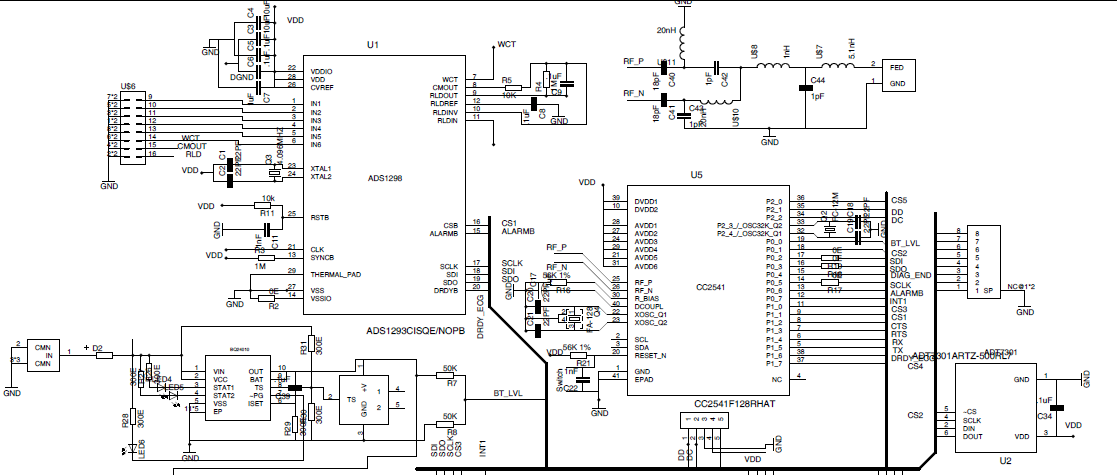
The bluetooth communication is functioning properly but I am getting all data as FF:FF:FF:FF......:FF:FF, after I removed the "if (send_buff != NULL)" condition. That means I am not getting any data from ADS1293. Secondly I examined the SPI communication between ADS1293 and CC2541 by writing a particular value to a register and reading it back continuously. I observed proper waveforms on SCLK,CS and MOSI pin, but nothing could be observed on MISO pin. That implies registers of ADS1293 are not written. I used the following code for testing SPI communication. I am also providing my schematic along with this. Please help me figure out the problem, I have been on this for quite a number of days but am unable find out the solution. Please help me out!
#define SPI_BAUD_M 0
#define SPI_BAUD_E 16


void spiWriteByte(uint8 write)
{
U0CSR &= ~0x02; // Clear TX_BYTE
U0DBUF = write;
while (!(U0CSR & 0x02)); // Wait for TX_BYTE to be set
}

void spiReadByte(uint8 *read, uint8 write)
{
U0CSR &= ~0x02; // Clear TX_BYTE
U0DBUF = write;
while (!(U0CSR & 0x02)); // Wait for TX_BYTE to be set
*read = U0DBUF;
}

void TI_ADS1293_SPIWriteReg(uint8 addr, uint8 value)
{
uint8 inst;

P1_1 = 0; // /CS enable

inst = 0X7F & addr; // register address
spiWriteByte(inst); // Send register address

spiWriteByte(value); // Send data value

P1_1 = 1; // /CS disable

}

uint8 TI_ADS1293_SPIReadReg(uint8 addr)
{
uint8 pVal, inst;

P1_1 = 0; // /CS enable

inst = 0X80 | addr; // register address

// WAIT_1_3US(2); // Wait
spiWriteByte(inst); // Send lower register address

spiReadByte(&pVal, 0xFF); // Read data

P1_1 = 1; // /CS disable

return pVal;

}


void main(void)
{


CLKCONCMD = (CLKCONCMD & ~(CLKCON_OSC | CLKCON_CLKSPD)) | CLKCON_CLKSPD_16M;


/***************************************************************************
* Setup I/O ports
*
* Port and pins used USART0 operating in SPI-mode are
* MISO (MI): P0_2
* MOSI (MO): P0_3
* SSN (SS) : P1_1
* SCK (C) : P0_5
*

*/


// Configure USART0 for Alternative 1 => Port P0 (PERCFG.U0CFG = 0).
PERCFG = (PERCFG & ~PERCFG_U0CFG) | PERCFG_U0CFG_ALT1;


// Set pins 2, 3 and 5 as peripheral I/O and P1_1 as GPIO output.
P0SEL = (P0SEL) | BIT5 | BIT3 | BIT2;
P1DIR |= BIT1;


/***************************************************************************
* Configure SPI
*/

// Set USART to SPI mode and Master mode.
U0CSR &= ~(U0CSR_MODE | U0CSR_SLAVE);

// Set:
// - mantissa value
// - exponent value
// - clock phase to be centered on first edge of SCK period
// - negative clock polarity (SCK low when idle)
// - bit order for transfers to LSB first
U0BAUD = SPI_BAUD_M;
U0GCR = (U0GCR & ~(U0GCR_BAUD_E | U0GCR_CPOL | U0GCR_CPHA | U0GCR_ORDER))
| SPI_BAUD_E;


/***************************************************************************
* Transfer data
*/

TI_ADS1293_SPIWriteReg(0x00,0x01);

int x;


while(1)
{

x = TI_ADS1293_SPIReadReg(0x00);

}

}