This thread has been locked.

If you have a related question, please click the "Ask a related question" button in the top right corner. The newly created question will be automatically linked to this question.

ADS1248 - How to test CMRR & NMRR

Other Parts Discussed in Thread: ADS1248, ADCPRO

Dear All,

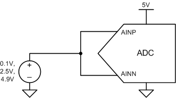
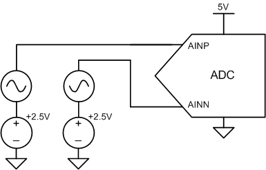
I would like to do a common & normal mode rejection test for ADS1248 on  RTD board design, with differential input configuration . This will help us to get an feel of testing and measuring the noise rejection value for our PCB with ADS1248 design. I need couple of support from Forum are mention below.

  1. How common mode rejection can be tested for PCB assembly?
  2. How normal mode rejection can be tested PCB assembly?
  3. With respect to what the common mode signal and normal mode signal are applied..?
  4. What kind of set up is required for above two tests. Can you provide simple setup diagram for above to tests
  5. How to quantify the noise rejection or the calculation steps for dB calculation.

Thanks And regards,

Dinu...

  • Dinu,

    I think this question has been asked of one of the FAEs supporting you and it was asked in an internal forum. I gave an answer earlier today, which I'll duplicate here. I've done a few tests just to test this out and I've got a few results.

    Originally, it was asked if there were any application notes on this subject. I don't know of any application notes on test circuits for our ADCs. However, most of the tests would be straight-forward, and not different than you might expect.

    For common mode rejection, I would assume you would use the internal reference for the ADC. The positive and negative inputs would be tied together and measurements would be made as the input was moved through the input range. Since the device has a digital filter with a frequency response that varies with data rate, I would do this as a DC test at whatever data rate is desired.

    As an example, for PGA=1, you would set AINP and AINN to 0.1V, 2.5V, and to 4.9V. This gives three measurements, one at the center of the common-mode input range, and the other two measurements at the edges of the common-mode input range. I would take 128 measurements at each input setting, and average each of the 128 measurement sets to separate the noise from the CMR measurement. In the end you'd have three sets of data converted to voltage: Data0.1, Data2.5, and Data 4.9.

    To get the CMR, you would calculate

    CMR = 20 * log ((2.4V)/|(Data2.5-Data0.1)|) and

    CMR = 20 * log ((2.4V)/|(Data4.9-Data2.5)|)

    and take the larger of the two as the CMR in dB. I used ADCPro with an ADS1248EVM and I got a value that was about 110dB. It's better than reported in the datasheet.

    With a different PGA value, you need to incorporate the gain into the calculation. As a second example, for a PGA=32, the input range is reduced because of the PGA. In our own testing, we do use slightly larger input range considering the gain (data is taken at +2.4V and +2.6V. Regardless, if your PGA gain is 32, input will vary less, given the PGA entire input and output range.

    It's also possible to take the endpoints of the CMR measurement in this example, I use endpoints, instead of taking the larger between variations from the midpoint.

    CMR = 20 * log ((32*0.2V)/|(Data2.6-Data2.4)|)

    With this measurement method, get something similar to that in the datasheet. In the end, it was close to 126dB

    For the normal mode rejection, it's another straight-forward measurement. In this one, you'd need a function generator with some DC offset so that the input would be in the center of the common-mode input range.

    I used an Agilent 33522A, which has two outputs, both are set to have a DC output of 2.5V. with 1Vpp and one 180° out of phase with each other. This gave me a ±1Vpp 50Hz signal. It also gave me a 1mV DC offset error, which I ignore for the AC measurement.


    Using two inputs that are 1Vpp and 180° out of phase gives me an ADC input that is 2Vpp as the input. Using ADCPro, I get this result:

    Which looks like I get a Vpp measurement of about 300uV. For this NMRR measurement the result is:

    NMRR = 20 * log (2V/300uV) = 76.5dB

    Which is a bit better than the expected value. Other measurements for 5Hz and 10Hz were a bit worse than expected. I got results that were about 95dB. Based on the output of the data, it looks as if the input has some extra low frequency noise. If I wanted to see the expected 110dB NMRR, I'd need to make sure the input signal noise (and input signal offset) would be less than the 40-50uV than I'm seeing. This might require extra input signal conditioning to clean up the signal source.

    I'm not sure I understand the last question about the noise rejection. In these examples, I've allowed the noise in the measurement and most have worked out fine. For the NMRR, test at 5SPS and 10SPS, the result is limited by the signal source and not the ADS1248.

    Regardless, I hope this is a good outline for the measurement. It's a standard set of measurements and it shouldn't be too difficult to test.

    Joseph Wu

  • Dear Joseph,

    Thanks for your reply, it helped me to understand how to perform the testing. 

    Regards,

    Dinu

  • Dinu,


    If you have a chance, I'd recommend getting an ADS1248EVM just to play with some of these tests (just as I've done in the explanation above). It's not hard to set up and it's a good way to see how the device operates.


    Joseph Wu
  • Hi Joseph,
    I have the board with me and could start with it and did bring-up. I have connected a 100ohms resistor(2 wire config) with a RBIAS of 2Kohm excitation current 1mA, gain = 1 enabled current excitation and tried reading the raw data @20SPS . I could read the data and found there is huge variation sample to sample.
    The sample to sample reading was not at all consistent but I was getting the reading what I soupose to get it was reading around 97mV. the sample to sample variation was around 150 counts.

    The I tried , shorting the differential input, configred the internal reference , gain = 1. I was expecting count near to zero plus the noise,but I was getting sample to sample count change around 40 counts. which is higher than the specified noise

    Operating condition:
    AIN0 shrt with AIN1
    Vref: 2.048V
    Res: 2^23
    Gain= 1
    Res in V= 0.24uV
    SPS = 20
    with out calibration
    so 40 count means nearly 10uV. do you have any idea what could be the reason.. what causing the sample to sample variation so high. if its a offset the 40 count , i could see a offset in the count as well.

    what is the expected sample to sample variation..?
    Please help.

    Regards,
    Dinu.
  • Dinu,


    Are you using the ADS1248EVM? Can you show your connections? I just want to make sure that the RBIAS and the measured resistor are connected correctly. The noise that you measure does seem rather high. Generally, the EVMs are fairly close to the noise performance in the datasheet.

    I can think of a couple of reasons that there might be extra noise. First, I would look for any extra device connections in the measurement or reference paths. If you are using the EVM, you may need to remove D1, D2, and D3. Those devices may have some leakage that could cause some extra drift. If you have your own board there might be some protection devices that could be causing the same type of leakage.

    Second, what precision resistors for the RBIAS and RTD are you using? If you have 1% resistors, you may be seeing the drift of the resistors. I would first start with using the highest precision resistors that you can easily get. Then I would try to shield the board so that there isn't a lot of air flow around the device, so the temperature will be consistent. If you are using the EVM, then the MMB0 may have some power dissipation that may slowly raise the temperature of the EVM, which may show a distribution in measurement.

    Lastly, you might have the measurement set up wrong. I want to make sure that you have a truly ratiometric measurement so that the reference of the ADC is only RBIAS times the excitation current as the reference. In this case, the current running through the RTD and RBIAS are exactly the same, so the ADC output is a ratio of the RTD/RBIAS values. Note that any current noise cancels out. If you have the measurement accidentally set so that the internal reference is routed to the REF0 pins, then any IDAC current noise reacting with the RTD is seen, while the IDAC current noise on RBIAS is masked because the internal reference is now driving the RBIAS. Make sure that the ADC uses REF0 as the reference, but the internal reference is not routed to REF0.

    I would also look at a set of long data (maybe 512 consecutive readings). Is there any periodic noise? Is there a long term drift? Seeing one or another may give a clue to where your noise (or other variance in data) is coming from. Since you're using 20SPS, it's unlikely that the line noise (50Hz or 60Hz) is affecting your measurement since the rejection is high at the data rate. If are able to record a set of raw data, I'd like to look at that.


    Joseph Wu
  • Dinu,


    You said that you were at Gain=1 and 20 SPS data rate, correct? Going back to the datasheet of the ADS1248, your expected rms noise would be about 2.62µV, and a peak-to-peak noise of 14.32µV. That would be greater than the 40 counts that you are getting now.

    I'm referring to Table 3 in the datasheet. There's a noise table of what you should expect.


    Joseph Wu