Because of the holidays, TI E2E™ design support forum responses will be delayed from Dec. 25 through Jan. 2. Thank you for your patience.

This thread has been locked.

If you have a related question, please click the "Ask a related question" button in the top right corner. The newly created question will be automatically linked to this question.

ADS1232 Linearity Issue

Other Parts Discussed in Thread: ADS1232REF, ADS1232

Hello fellow Engineers,

I have been designing analog circuits for about 20 years, and I can say that I am about stumped.  I would sincerely appreciate your help/input.

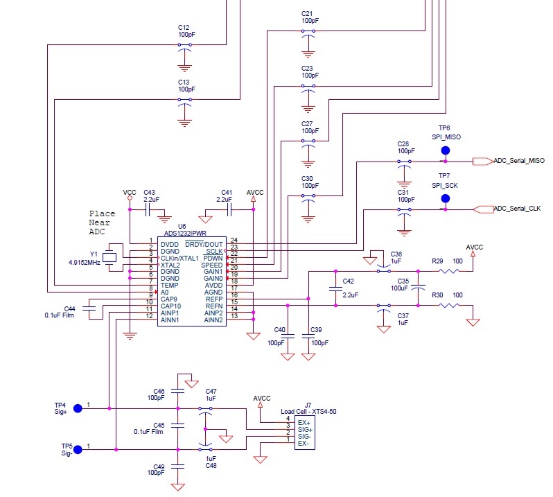
I am using an ADS1232 and have basically taken the front end circuit from the Evaluation board (ADS1232REF).  The exact circuit I am using is below:

For full disclosure, I am using a Common-Mode choke (Murata-DLW5BTM102TQ2K) to separate the Analog supply from the Digital.

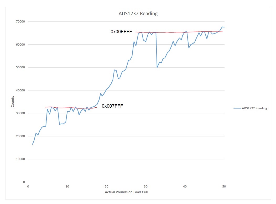
My issue is really unusual.  My analog input off of the load cell (in mV) is perfectly linear all the way up to the chip pins.  Once the signal gets into the chip, it is a different story.  The digital output is having issues "rolling over" to the next Most Significant Bit.  It will roll over from 0x003FFF to 0x004000.  It seems to be linear up until about 0x005FFF.  It will roll over from 0x005FFF to 0x007***, and fumble around with the bits while the pressure rises up to 0x007FFF and then it will double back to 0x007C00 until you finally run it up to 0x007FFF again, and then the MSB will finally increment so that you get 0x008000.  After this, it seems to be linear up to 0x00EFFF and then it strays from the path again between 0x00FFFF.  Eventually it will roll over to 0x010000, but this is about the limit of my load cell.

I have hard-wired an external reference voltage into it with no success.  I have changed the input capacitor (C45) with no change, but the signal is fine there on a scope or DVM.  I've tried changing the gain and the speed with no success.  I initiate a zero offset calibration at start-up and don't again after that.  Again, I am using the same components as on the demo board for the most part.

I would appreciate the input on this issue.  I have ordered an ADS1232REF to evaluate against my circuit, in case there is a difference.

Thanks so much for the input!!!

Cheers!

Jonathan

Honortronics Inc.

  • Hi Jonathan,

    The first thing I would do is remove the choke from in front of the analog supply.  If you want some filtering I would replace the choke and add a simple RC filter with a 2 ohm resistor and add additional capacitance to AGND.  In general we have seen a number of issues related to inductance on the supply lines.  There are times when the ADC will increase current demands and the choke will do it's job and choke the current in those short duration demands.

    Also, you should have as low inductance as possible between AGND and DGND at the device pins.  Any short duration pulse on an inductive path (to include long PCB traces) between the grounds can potentially separate the two grounds my more than 300mV which will then exceed the absolute maximum rating for the ADS1232 and damage the part.

    Would you also send us the pin settings you are using with respect to Gain, Speed, etc. so we can examine this further?  Also sending us collected data showing the issue as presented may also point something out to us.

    Best regards,

    Bob B

  • Hey Bob,

    Thanks so much for your reply.  You were spot-on in your assessment of what I should look into next, unfortunately it still hasn't solved my problem yet.  This is an unusual enough problem to be attributed to decoupling or ground loops, or some other "black art".

    Below is the resulting curve from my tests incrementing the load in 1/2# increments.  This is showing how it is doubling over.

    I have done about as much as I can think of with your advice.  I removed the choke and jumped it.  I jumped just the GND side, and I also jumped just the GND side, but installed a 33uF Tantalum capacitor at that junction.  This didn't make any difference.  I also added a 0.1uF and a 0.01uF ceramic capacitor in parallel with the 2.2uF capacitors for the decoupling for both supplies.  These are placed very close to the power pins for the chip.  I removed the ground jump from where I jumped the missing choke, and I added a single ground merge right at the ADC power pins so that was the only place they came together to eliminate all possibility of potential between them...it still didn't work.  I added the 33uF Tantalum cap there for fun to see if it would help, and it did not.  I removed the analog supply all together and added an external supply, which didn't solve the problem.

    For these measurements, I am running the system in a gain of 1 (Gain0 & Gain1 = Low). and the speed is low to get 10Hz.  Obviously I am running an external crystal, but I have also jumped the clock-in to ground to activate the internal oscillator, and this didn't make a difference.

    I am attaching the raw Excel file with the data if you would like to check it out.  Again, I would sincerely appreciate the input here.  I am really pulling out all the stops (so I believe) to get this working and am coming up with Nil so far.  Thanks again.

    Sincerely,

    Jonathan

    LinearityExample_16-11-14.xlsx

  • Hi Jonathan,

    Just so I'm totally clear, you actually have the load cell connected and not a simulator, correct?  And the load cell you are using has a sensitivity of 3mV/V?  And what is the excitation voltage?

    Is there some reason why you are using a gain of 1 as opposed to 64 or 128?  At a gain of 1 the PGA is bypassed lowering the input impedance.  As the data are appearing as a single point, I'm not sure if you have settled data or if you are averaging or doing any post processing to the data.  The digital filter requires a number of conversion cycles before the output is settled.  So, after the weight has changed you should throw away 4-5 conversions.

    From the data it appears that there is a considerable amount of offset.  From rough calculation I would expect about 1000 codes per gram.  Your starting weight of about 1 gram shows 16k codes.  This is very unusual to have this much offset which is about 1/3 of the scale output.  The load cell itself has an offset of about 1%, and 500 codes is a long way from 15000.  It is not clear as to what is causing this offset unless there is some loading from the lower impedance of the ADC.

    The next steps I would take is to make absolutely sure there is no inductance on AVDD (which includes ferrites), change the Gain to 128 (or at least 64), and make sure that the data are full settled before taking a reading.

    Best regards,

    Bob B

  • Hi Jonathan,

    Some further comments.  I looked again at the design information and the input impedance at a gain of 1 or 2 should still be pretty high as this stage uses a pre-charge buffer.  So this confuses me further as to why there is so much offset.  One thing to reiterate is the pre-charge buffer will demand periodic peak currents and will vary depending on the actual input voltage.  If the current is being choked during these times, the result may also vary.

    I was a little confused by your comments on what you said you tried.  If you applied an external supply that went through an inductive path you need to revise the circuit pathway to remove any inductance on the AVDD supply path. We have seen in multiple cases where any inductance on the ADS1232 supplies, and in particular the analog supply, will cause odd problems to occur.

    Best regards,

    Bob B

  • Hello again, Bob.

    I have been diligently working on this project since our correspondence and I have identified the issue.  To cut to the chase, the "silver bullet" was when I removed the choke, and instead of just jumping the choke, I had to move the ground merge to a wire that was right over top of the ADS1232.  With that as the ground merge, the problem went away.  Here is a chart with the compilation of the results:

    To answer your questions, I have done all of my testing in the real world.  I am using an actuator to push a spring that is attached to a scale, and I have a load cell on the end of the actuator telling me how hard it is pushing.  I have a microcontroller keeping track of all of this, so I am running it on a debugger the whole time.  I am pausing the execution after I get to my set-point and recording the results that are in the actual registers.

    Since it was still within the linear range, I increased the gain to x64, which also helped.  I did all of my testing at that gain setting.

    Again, I sincerely appreciate your input on this, Ben.  Your saying "odd problems" resulting in differences in potential across the grounds turns out to practically be an understatement.  My choke was only about 3/8" away from the ADC, so I was genuinely surprised when moving the ground merge that small of a distance made such an enormous difference in the results.  Results are results, so in hopes to benefit my fellow engineers, I post the results of my testing.