This thread has been locked.

If you have a related question, please click the "Ask a related question" button in the top right corner. The newly created question will be automatically linked to this question.

ADS8332: Layout guideline for TSSOP package

Part Number: ADS8332

Dear Team,

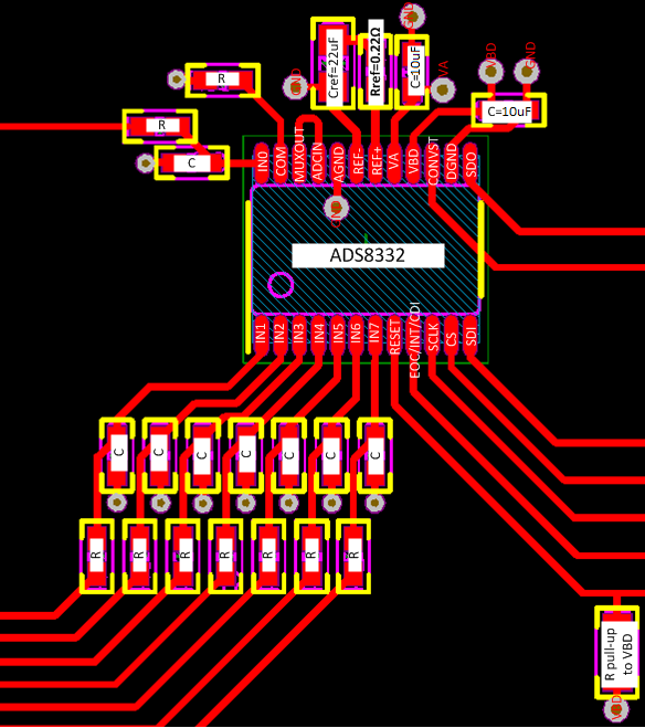
My customer would like to use ADS8332 on their new design. They prefer to use TSSOP package and they need a layout guideline for this package. datasheet and EVM documents have guidelines for only QFN package.

Do you have a guideline for TSSOP package as well?

Best regards,

Caglar

  • Hi Caglar,

    The general SAR ADC layout guidelines used for the QFN package will also apply to the TSSOP.  Please see below.  I don't immediately have a TSSOP layout plot, but will post an example by tomorrow.

    Thank you,

    Kind Regards,

    Luis Chioye

    • The power sources to the device must be clean and well-bypassed.
    •  Use 10 μF, ceramic bypass capacitors in close proximity to the analog (VA) and digital (VBD) power-supply pins.
    • Avoid placing vias between the AVDD and DVDD pins and the bypass capacitors.
    •  Connect all ground pins to the ground plane using short, low impedance paths.
    • The REF+ reference input is bypassed with a 22 μF, X7S-grade, 0805-size, 10-V rated ceramic capacitors.
    •  Place the reference bypass capacitor as close as possible to the reference REF+ and REF- pins and connect the bypass capacitor using short, low-inductance connections.
    • Avoid placing vias between the REF+ and REF- pins and the bypass capacitor.
    •  If the reference voltage originates from an op amp, make sure that the op amp can drive the bypass capacitor without oscillation. A small 0.2-Ω to 0.5-Ω resistors (RREF) is used in series with the reference bypass capacitor to improve stability.

  • Hi Caglar,

    Please find below a plot of a TSSOP ADS8332 layout for reference. Please find below the layout recommendations:

    • Partition the PCB into analog and digital sections. Care must be taken to ensure that the analog signals are kept away from the digital lines. This layout helps keep the analog input and reference input signals away from the digital noise. In this layout example, the analog signals are routed on the left side of the board and the digital connections are routed on the right side of the board
    • Using a single common ground plane is strongly recommended. For designs requiring a split analog and digital ground planes, the analog and digital ground planes must be at the same potential joined together in close proximity to the device.
    • Power sources to the ADS8332 must be clean and well-bypassed. As a result of dynamic currents during conversion, each supply must have a decoupling capacitor to keep the supply voltage stable. Use wide traces or a dedicated analog supply plane to minimize trace inductance and reduce glitches.The power sources to the device must be clean and well-bypassed.
    • Use 10 μF, ceramic bypass capacitors in close proximity to the analog (VA) and digital (VBD) power-supply pins.
    • Avoid placing vias between the AVDD and DVDD pins and the bypass capacitors.
    • Connect all ground pins to the ground plane using short, low impedance paths.
    • The REF+ reference input is bypassed with a 22 μF, X7S-grade, 0805-size, 10-V rated ceramic capacitors.
    • Place the reference bypass capacitor as close as possible to the reference REF+ and REF- pins and connect the bypass capacitor using short, low-inductance connections.
    • Avoid placing vias between the REF+ and REF- pins and the bypass capacitor.
    • If the reference voltage originates from an op amp, make sure that the op amp can drive the bypass capacitor without oscillation. A small 0.2-Ω to 0.5-Ω resistors (RREF) is used in series with the reference bypass capacitor to improve stability.

    Thank you and Best Regards,

    Luis Chioye