Part Number: ADS1148-Q1
Other Parts Discussed in Thread: TMS320F28377D, ADS1148
Hello all,
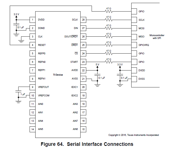
I am working on this ADC with TMS320F28377D for SPI communication. I am having issue in code as after sending read data command and clock command, I am getting the value '0' in results but it should be having the value of the applied input. Data ready interrupt is coming and commands are transferred accordingly. In the inputs I am applying 2.3V on AIN0 pin and 1.65V(Vcm) on AIN1 pin. Please help me with the issue below is attached the code.
//
#include "F28x_Project.h"


//
// Function Prototypes
//

interrupt void SPIA_TX_ISR(void);
interrupt void SPIA_RX_ISR(void);
void delay_loop(void);
void spi_init(void);
void error();
void SPITX_INTERRUPT_Service();
void adc_enable();
void Sdata_command();
void Wreg_command1();
void Wreg_command2();
void Wreg_command3();
void Wreg_command4();
void Wreg_command5();
void Wreg_command6();
void Rreg_command1();
void Rreg_command2();
void Sync();


int i, index, adc_flag, SPI_TX_RX, j, toggle=0;


void main(void)
{

//
// Step 1. Initialize System Control:
// PLL, WatchDog, enable Peripheral Clocks
// This example function is found in the F2837xD_SysCtrl.c file.
//
	InitSysCtrl();

//
// Step 2. Initialize GPIO:
// This example function is found in the F2837xD_Gpio.c file and
// illustrates how to set the GPIO to it's default state.
// Setup only the GP I/O only for SPI-A functionalitys
//

	InitGpio();
	GPIO_SetupPinMux(59, GPIO_MUX_CPU1, 0);                      //drdy  110
	GPIO_SetupPinOptions(59, GPIO_INPUT, GPIO_PULLUP);

	InitSpiaGpio();


	XintRegs.XINT1CR.all = 0x0000;					  // XINT4 disable
	XintRegs.XINT1CR.bit.POLARITY = 00;				  // 01: Interrupt is selected as positive edge triggered
	XintRegs.XINT1CR.bit.ENABLE = 1;

	InputXbarRegs.INPUT4SELECT = 40;

	PieCtrlRegs.PIEIER1.bit.INTx4 = 0;				//Disable XINT1 int.
	PieCtrlRegs.PIEIFR1.all = 0;


// Step 3. Initialize PIE vector table:
// Disable and clear all CPU interrupts
//
	DINT;
	IER = 0x0000;
	IFR = 0x0000;

//
// Initialize PIE control registers to their default state:
// This function is found in the F2837xD_PieCtrl.c file.
//
	InitPieCtrl();

//
// Initialize the PIE vector table with pointers to the shell Interrupt
// Service Routines (ISR).
// This will populate the entire table, even if the interrupt
// is not used in this example.  This is useful for debug purposes.
// The shell ISR routines are found in F2837xD_DefaultIsr.c.
// This function is found in F2837xD_PieVect.c.
//
	PieCtrlRegs.PIECTRL.bit.ENPIE = 0;     // Enable the PIE block
	PieCtrlRegs.PIEACK.all = 0xFFFF;
	PieCtrlRegs.PIEIER6.bit.INTx1 = 1;     // Enable PIE Group 6, INT 1
	PieCtrlRegs.PIEIER6.bit.INTx2 = 1;     // Enable PIE Group 6, INT 2
	PieCtrlRegs.PIEIER1.bit.INTx4 = 1;     // Enable PIE Group 1, INT 4
	PieCtrlRegs.PIEIFR6.all = 0;

	InitPieVectTable();

//
// Interrupts that are used in this example are re-mapped to
// ISR functions found within this file.
//
		EALLOW;
		// This is needed to write to EALLOW protected registers
		PieVectTable.SPIA_RX_INT = &SPIA_RX_ISR;
		PieVectTable.SPIA_TX_INT = &SPIA_TX_ISR;
		EDIS;
	    // This is needed to disable write to EALLOW protected registers

//
// Step 4. Initialize the Device Peripherals:
//
	spi_init();   // Initialize the SPI only
	for (i = 0; i < 32000; i++);
	GPIO_WritePin(19, 0);


// Enable Global Interrupts

//
// Step 5. User specific code, enable interrupts:
//


//
// Enable interrupts required for this example

	IFR = 0x00;
	IER = 0x21;                                     // Enable CPU INT1, INT6
	EINT;
	PieCtrlRegs.PIEACK.all = 0xFFFF;				//Clear all ACK bits before starting back ground loop.

	for (i = 0; i < 32000; i++);                    //16ms
	adc_flag=1;
	index=1;
	adc_enable();

//
// Step 6. IDLE loop. Just sit and loop forever (optional):
//
	for (;;);
}

//
// error - Function to halt debugger on error
//
void error(void)
{
	asm("     ESTOP0");                             //Test failed!! Stop!
	for (;;);
}

//
// spi_fifo_init - Initialize SPI FIFO
//
void spi_init()
{
	 EALLOW;

		   SpiaRegs.SPICCR.bit.SPISWRESET = 0;     	// 7    SPI SW Reset
		   SpiaRegs.SPICCR.bit.SPICHAR = 0x7;	 	//      Character length of 8-bits.To facilate insturction code and data bytes of EEPROM.
		   SpiaRegs.SPICCR.bit.SPILBK     = 0;     	// 4    Loop-back is disable.
		   SpiaRegs.SPICCR.bit.CLKPOLARITY= 0;     	// 6    Data is shifted out on falling edge of clock.And recieved on
		   						        		    //       rising edge of clk to make compatibility with EEPROM.
		   SpiaRegs.SPIBRR.all = 0x0063;            //       Baud rate
		   SpiaRegs.SPICTL.bit.SPIINTENA    = 1;    // 0      Interrupts(SPIRXINT & SPITXINT)are enable.
		   SpiaRegs.SPICTL.bit.TALK         = 1;    // 1      Slave transmit is enable for EEPROM but must be
		   										    //        stop in case of DAC writting or donot read Rx for DAC.
		   SpiaRegs.SPICTL.bit.MASTER_SLAVE = 1;    // 2      SPI work as master.
		   SpiaRegs.SPICTL.bit.CLK_PHASE    = 1;    // 3      Output Data on clock.
		   SpiaRegs.SPICTL.bit.OVERRUNINTENA= 0;    // 4      Overrun interrupt is Disable as there is complete control on EEPROM. and no data from DAC.

		   SpiaRegs.SPIRXEMU	= 0x0000;		    // Dummy of SPIRXBUF clear to zero.
		   SpiaRegs.SPITXBUF	= 0x0000;		    // SPITXBUF clear to zero.
		   SpiaRegs.SPIRXBUF	= 0x0000;		    // SPIRXBUF clear to zero.
		   SpiaRegs.SPIDAT		= 0x0000;		    // clear initially to zero.
           SpiaRegs.SPIFFTX.bit.SPIFFENA   = 0;	    //FIFo Feature is Disabled.
		   SpiaRegs.SPIPRI.bit.FREE    = 1;         // 4      Free emulation mode control is selected.
		   SpiaRegs.SPIPRI.bit.SOFT    = 1;         // 5      Soft emulation mode control is selected.
		   SpiaRegs.SPICCR.bit.SPISWRESET = 1;      // 7      SPI SW Out of reset.

		EDIS;
}

//
// spiTxFifoIsr - ISR for SPI transmit FIFO
//
interrupt void SPIA_TX_ISR(void)
{}

void SPITX_INTERRUPT_Service()
{
	j = SpiaRegs.SPITXBUF;              // TRANSMIT data

	if (index == 1 && adc_flag == 1)
	{
		adc_enable();
	}

	else if (index == 2)
	{
		Sdata_command();
	}

	else if (index == 3)
	{
		Wreg_command1();		      // Address of first register
	}

	else if (index == 4)
	{
		Wreg_command2();		     // Number of bytes to be written
	}

	else if (index == 5)
	{
		Wreg_command3();
	}

	else if (index == 6)
	{
		Wreg_command4();
	}

	else if (index == 7)
	{
		Wreg_command5();
	}
	else if (index == 8)
	{
		Wreg_command6();
	}

	else if (index == 9)
	{
		Rreg_command1();
	}

	else if (index == 10)
	{
		Rreg_command2();
	}

	else if (index == 11)
	{
		Sync();
	}

}

void adc_enable()
{

	//GPIO_WritePin(51, 1);					 //Start pin of ADC is applied 3.3v directly
	asm(" NOP");
	asm(" NOP");
	asm(" NOP");
	GPIO_WritePin(19, 0);                    // Set CS low
	asm(" NOP");
	asm(" NOP");
	asm(" NOP");
	//GPIO_WritePin(49, 0);                  //Reset pin of ADC is applied 3.3v directly
	SPI_TX_RX = 1;
	SpiaRegs.SPIDAT = 0x06;
	index = 2;
}

void Sdata_command()
{
	for (i = 0; i < 12000; i++);            //0.6 ms
	SpiaRegs.SPIDAT = 0x16;			        // SDATAC command
	index = 3;
}

void Wreg_command1()
{
	SpiaRegs.SPIDAT = 0x40;
	index = 4;
}

void Wreg_command2()
{
	SpiaRegs.SPIDAT = 0x03;
	index = 5;
}

void Wreg_command3()
{
	SpiaRegs.SPIDAT = 0x01;
	index = 6;
}

void Wreg_command4()
{
	SpiaRegs.SPIDAT = 0;
	index = 7;
}

void Wreg_command5()
{
	SpiaRegs.SPIDAT = 0;
	index = 8;
}

void Wreg_command6()
{
	SpiaRegs.SPIDAT = 0x04;
	index = 9;
}

void Rreg_command1()
{
	SpiaRegs.SPIDAT = 0x20;
	index = 10;
}

void Rreg_command2()
{
	SpiaRegs.SPIDAT = 0x03;
	index = 11;
}

void Sync()
{
	SpiaRegs.SPIDAT = 0x04;
	for (i = 0; i < 40; i++);                  //1.78 us
	index = 12;

}

interrupt void SPIA_RX_ISR(void)
{
	i = SpiaRegs.SPIRXBUF;                    // Read data

   if (SPI_TX_RX == 0)
	{}
	else
	{
		SPITX_INTERRUPT_Service();
	}

	SpiaRegs.SPIFFRX.bit.RXFFOVFCLR = 1;      // Clear Overflow flag
	SpiaRegs.SPIFFRX.bit.RXFFINTCLR = 1;      // Clear Interrupt flag
	if(toggle ==1)
	{
		toggle = 2;
		SpiaRegs.SPIDAT = 0;                  // Read for clock
	}
	PieCtrlRegs.PIEACK.bit.ACK6 = 1;
}

interrupt void XINT1_ISR(void)
{
	PieCtrlRegs.PIEACK.bit.ACK1 = 1;
	GPIO_WritePin(19, 0);
	asm(" NOP");
	asm(" NOP");
	asm(" NOP");
	if(toggle == 0)
	{
		toggle = 1;
		SpiaRegs.SPIDAT = 0x12;              //READ
	}
	else if(toggle == 2)
	{
		toggle = 0;

	}
	asm(" NOP");
	asm(" NOP");
	asm(" NOP");
	for (i = 0; i < 40; i++);
}
Regards,
Ami