This thread has been locked.

If you have a related question, please click the "Ask a related question" button in the top right corner. The newly created question will be automatically linked to this question.

DAC8822: About the "settling time" of DAC8822 vs. AD5547

Part Number: DAC8822
Other Parts Discussed in Thread: THS4011

Dear expert,

Here is a question about the "settling time" of DAC8822 vs. AD5547.

1, From the datasheet, we can see both DAC8822 and AD5547 have the same spec - 0.5us settling time.

2, But in real application, my customer designed their board with DAC8822 and they tested the settling time is around 0.2us, but their competitor designed the board with AD5547 and they tested the settling time is exact 0.5us. (the schematic/pcb are not the same)

question:

what is the key factor for the settling time? 

how to get the smaller settling time in the system design with DAC8822?

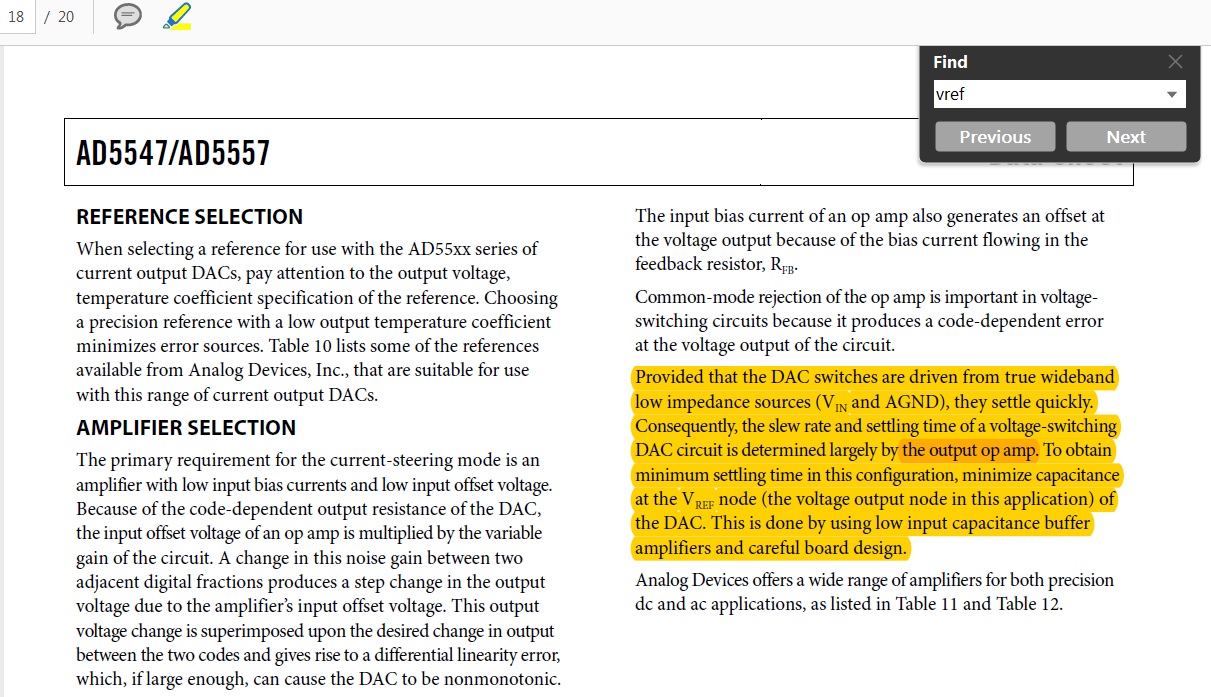
3, I just checked the AD5547 datasheet, they mentioned that to obtain the minimum settling time in this configuration, minimize capacitance at the Vref node of the DAC. this is done by using low input capacitance buffer amplifiers.

Question: could you please help comments on where is the location of this low input capacitance buffer they mentioned?

Best Regards

Iven Xu

  • Hello Iven,

    The Engineer who primarily supports these products is located in India and will be observing the local Independence Day holiday tomorrow. I will temporarily help out here until his return.

    Is it possible for us to look at schematic details fro this design? Specifically at least understanding the output amplifiers used in each the DAC8822 and AD5547 designs is imperative. Both of these products are MDACs which means they will either need a transimpedance amplifier on the IOUT pin to derive a voltage output, or (to the ends that the ADI text is discussing) in a configuration resembling an R-2R DAC where the system is used in "reverse" (reference voltage applied at IOUT and output derived at VREF) - in this case a buffer amplifier is placed at the VREF node. We have TI Designs explaining both:

    - MDAC Transimpedance Design (www.ti.com/.../TIPD137)
    - MDAC "R-2R" Design (www.ti.com/.../TIPD159)

    The slew-rate and input capacitance of the output buffer will directly impact the settling time. As the DAC8822 datasheet indicates, the settling time data was collected using the THS4011 as the transimpedance amplifier in the more "typical" MDAC configuration. We need to understand their setup to contrast their observations versus what is in the datasheet.
  • Hello Kevin,

    thanks very much for your prompted response.
    pls let me double check with customer then back to you guys again for the further discussion.


    Best Regards
    Iven Xu
  • Hello Kevin

    I have shared customer's schematic through email. could you please help check and comments? thanks.

    Best Regards
    Iven Xu