This thread has been locked.

If you have a related question, please click the "Ask a related question" button in the top right corner. The newly created question will be automatically linked to this question.

ADS114S06B: Please Help! I can't get correct data from my ADC...

Part Number: ADS114S06B

Please Help! I can't get correct data from my ADC...


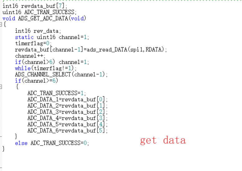
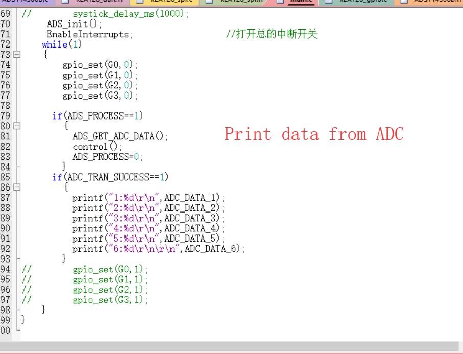
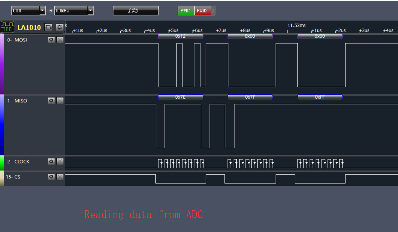
I am using ADS114S06B for my smart car application.But I cant get correct data from ADC,I connect all the ADC input to GND. And Pin 23 is output with 2.5V.

  • Hi user 5771857,

    Welcome to the E2E forum! There are a couple of issues in the logic analyzer sequences. The first is with the read data sequence. CS is toggling between bytes transmitted which resets the SPI internal circuitry within the ADS114S06B and cancels the communication. CS must stay low throughout the entire communication transaction.

    Second issue is with the register write command. The command is issuing a write to two registers (0x02 and 0x03) with the contents of 0x0C. For the register 0x02 the INPMUX register is set to AIN0 and AINCOM. Are you sure that AIN0 is at ground? Also, for the contents of register 0x03 the PGA setting is incorrect. 0x0C is PGA enabled at a gain of 16. Ground is outside of the input range of the device with PGA enabled, so the proper setting would be 0x00 which is PGA powered down and bypassed and using a gain of 1.

    You need to verify that the communication is working as needed and that the commands are correct in the logic analyzer plots.

    In the ADS_init() function you have an number of commands sent back to back followed by the RESET command. First thing is the commands all take time to complete so you must have a delay between commands if you use them. Second, RESET will reset any of the previous actions to the default device conditions. Third, the system gain and offset calibration commands require specific input conditions. For example, the system gain cal requires a full-scale voltage value input to the ADS114S06B. You should do the RESET command first followed by a delay. Then only issue the self offset calibration command. You can use the system calibration commands, but if you do review section 9.3.12 in the datasheet on page 40.

    In your schematic you have connected the NC pin (25) of the device. NC means no connect.

    Best regards,
    Bob B
  • Hello Bob B,
    Thank you for your analyze, I will trying my best to reprogram my device and test it.
    Here is PGA set up:

    void ADS_CHANNEL_SELECT(uint16 channel)
    {
    uint8 channel_MASK;
    channel_MASK = 0x0c;
    switch(channel)
    {
    case 0:
    channel_MASK |= 0x00;
    ads_write_REG(spi1,ADS_WRITE_FIRSTBITE_MASK | INPMUX,channel_MASK);
    break;
    case 1:
    channel_MASK |= 0x10;
    ads_write_REG(spi1,ADS_WRITE_FIRSTBITE_MASK | INPMUX,channel_MASK);
    break;
    case 2:
    channel_MASK |= 0x20;
    ads_write_REG(spi1,ADS_WRITE_FIRSTBITE_MASK | INPMUX,channel_MASK);
    break;
    case 3:
    channel_MASK |= 0x30;
    ads_write_REG(spi1,ADS_WRITE_FIRSTBITE_MASK | INPMUX,channel_MASK);
    break;
    case 4:
    channel_MASK |= 0x40;
    ads_write_REG(spi1,ADS_WRITE_FIRSTBITE_MASK | INPMUX,channel_MASK);
    break;
    case 5:
    channel_MASK |= 0x50;
    ads_write_REG(spi1,ADS_WRITE_FIRSTBITE_MASK | INPMUX,channel_MASK);
    break;
    }

    }

    void ADS_SELECT_PGA(uint16 PGAs)
    {
    if(PGAs<=1) ads_write_REG(spi1,ADS_WRITE_FIRSTBITE_MASK | PGA,0x00);
    switch(PGAs)
    {
    case 2:
    ads_write_REG(spi1,ADS_WRITE_FIRSTBITE_MASK | PGA,0x09); //2X
    break;
    case 3:
    ads_write_REG(spi1,ADS_WRITE_FIRSTBITE_MASK | PGA,0x0a); //4X
    break;
    case 4:
    ads_write_REG(spi1,ADS_WRITE_FIRSTBITE_MASK | PGA,0x0b); //8X
    break;
    case 5:
    ads_write_REG(spi1,ADS_WRITE_FIRSTBITE_MASK | PGA,0x0c); //16X
    break;
    case 6:
    ads_write_REG(spi1,ADS_WRITE_FIRSTBITE_MASK | PGA,0x0d); //32X
    break;
    case 7:
    ads_write_REG(spi1,ADS_WRITE_FIRSTBITE_MASK | PGA,0x0e); //64X
    break;
    case 8:
    ads_write_REG(spi1,ADS_WRITE_FIRSTBITE_MASK | PGA,0x0f); //128X
    break;
    }


    }


    Best wishs,
    Harry.
  • Is there any influence to connect NC to GND?
  • Hi Harry,

    The datasheet recommends leaving this pin not connected or alternately can be tied to AVSS.  If AVSS is at GND then this connection is ok.

    Bests regards,

    Bob B