This thread has been locked.

If you have a related question, please click the "Ask a related question" button in the top right corner. The newly created question will be automatically linked to this question.

ADS8330: SCLK TAG bit, and SDI signal 1101

Part Number: ADS8330

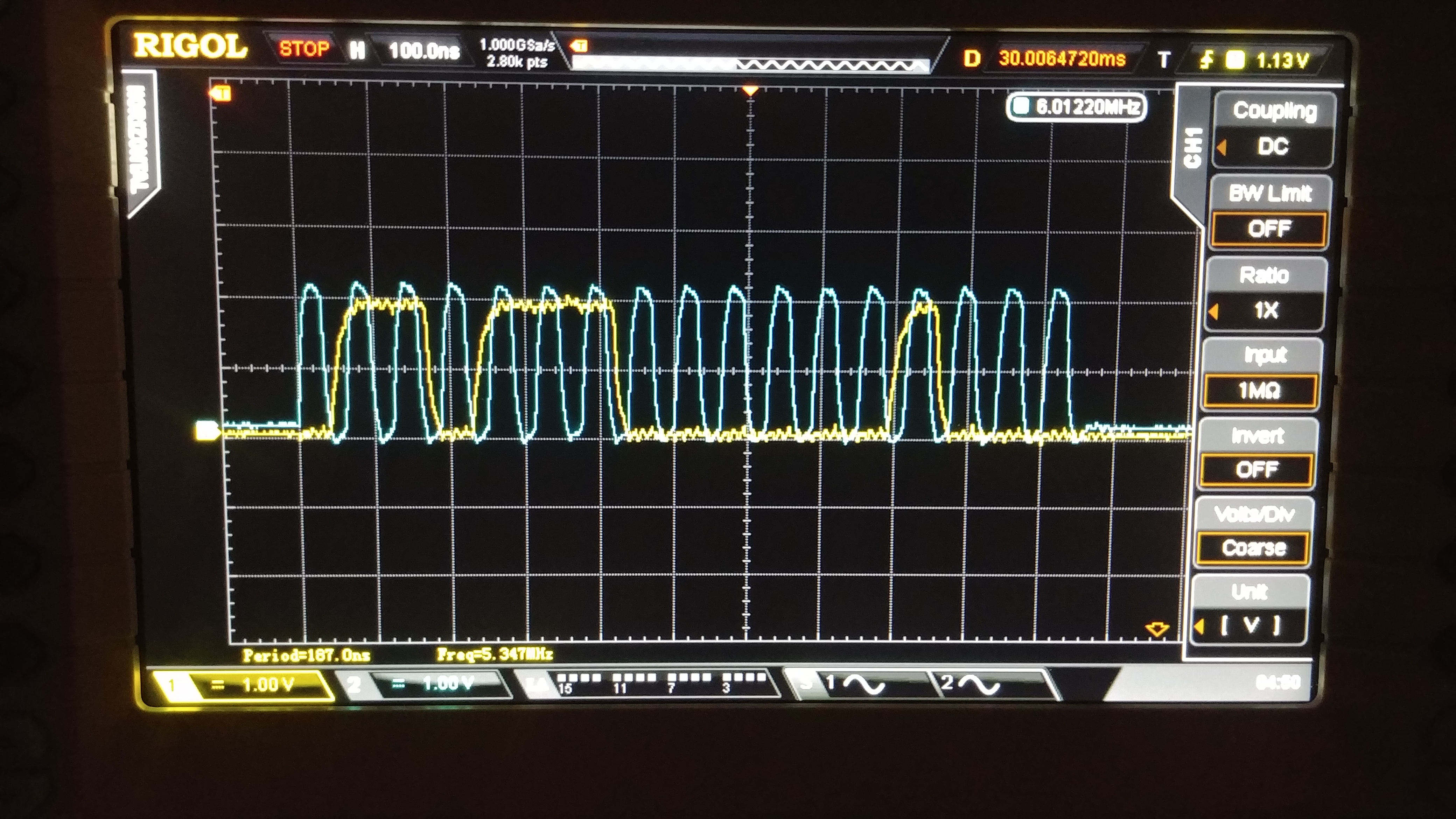
We are getting data out of this chip, but there seems to be issues with the data.  Mostly, the last three bits coming out are nearly all 100, effectively reducing the 16-bit resolution to 13-bit.  Before we go to the trouble of reconfiguring the system, I wanted to know if any of the following creates any known issues, or if it should work OK in this manner.

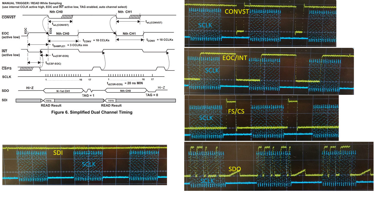
For TAG use, I would like to know if the 17 SCLK pulses can simply be all spaced at the same interval or if there needs to be a space between the 16th and 17th pulse.  The datasheet Figures (such as Figure 6) show 16 pulses on SCLK, a small space, then the 17th pulse, but this small space is not documented anywhere that I can find.

Also, one of our engineers configured the SDI signal to remain essentially always high, there is no 1101 that coincides with the first 4 pulses of the SCLK pulse stream.  Does this create a problem?  Or does the SDI pin really need the 1101 to properly function?  The SDI only has a zero for an occasional reset, but during data read-out, the SDI signal is always high.  This seems to conflict with the datasheet showing a 1101 is needed, but the engineer that configured it this way is claiming that since we are getting data out, it should be fine.  I'm wondering if this could be affecting the timing, however, and maybe contributing to our strange issue of nearly all data ending in 100.

One other strange thing we see is what appears to be a data anomaly when the 15th and 16th bits flip (right at the mid-point).  Our data seems stretched in this region - sinusoids for example show elongation near this value, and I'm wondering if the above issues may also be causing this.  The elongation is on the order of 3-bits (8 counts).  It's very obvious if for example the tip of a sinusoid barely crosses the midpoint.

  • I should mention we are using the default configuration.  Here are the timing signals, in comparison with Figure 6.

  • Hello Robert,

    There are no timing restrictions between the 17th pulse and the TAG bit. Also, writing 1101 is not exclusive to reading the conversion result. The conversion results are always shifted out except when reading the CMR register. If you just want to use the default configuration, it is perfectly valid to tie SDI to the +VBD pin.

    The convert start and /CS waveforms relative to SCLK look fine. Can you send a zoomed in waveform of SCLK and SDO, along with the scope settings? I want to make sure the timing requirements are met. The SDO seems to have a slow rise time from the picture that you sent.

    Thank you,
    Keith N.
    Precision ADC Applications
  • The SDO does have a slow rise time, but we are getting the data as shown.

    Here is a zoomed in version of SCLK (cyan) with SDO (yellow).

    Notice the last three bits are 100 - this is the big problem we have - I'd say about 19/20 words come out ending in 100.  Of the 1/20 words that don't, nearly all of those end 110.  It is very rare to get the last 3 bits to show a value any different, so effectively we aren't getting the full (needed) 16 bits.

    Scope settings are 100ns per division, 1V per division.  I have the two waveforms slightly offset vertically to make it easier to see where the transitions occur.

  • I purchased a couple new chips and they work fine. I think we must have received a bad batch of chips that caused these issues.
  • Hi Robert,

    I am glad you have it working. I do not see any timing violations, so this is likely due to a damaged part. I have not seen this exact behavior before, but it is possible there is higher than normal internal leakage as a result of mild ESD damage.

    In any case, it looks like you are able to move forward with your project.

    Thank you,
    Keith N.
  • So, in summary, the timing above is all OK, although not documented well in the datasheet.

    We just discovered what was causing the last 3 bits to behave in the strange manner - the chips were not damaged (a surprise!).  The capacitors on the voltage rails were all well under recommended values, so when those were fixed, the chip was behaving well.

    This was also causing the erroneous data we saw near the mid-point (15th and 16th MSBs flip).

    I know a lot of chips come with recommendations for 0.1 uF caps on the supply voltage, and what happened here was an oversight that the supply voltage for this chip needs much more substantial capacitance.

  • Thank you for the feedback!
    Regards,
    Keith N.