This thread has been locked.

If you have a related question, please click the "Ask a related question" button in the top right corner. The newly created question will be automatically linked to this question.

DLP2021-Q1: DLP2021 Power up sequence

Part Number: DLP2021-Q1
Other Parts Discussed in Thread: TPS65100, , AM2632

Tool/software:

Hello TI, 

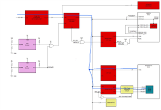
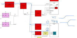
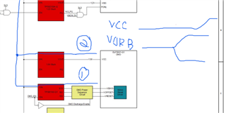
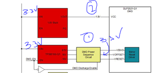
We are using LDO TPS6285018AQDRLRQ1 for 1.8V generation and TPS65100 chip for Voffset , Vbias and Vreset Voltages  generation.

We have same Supply 3.3V available at input for both LDO TPS6285018AQDRLRQ1 for 1.8V generation and TPS65100 chip.

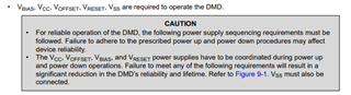
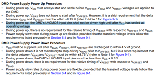
We have issue during power up sequence , that 3.3V available at Voffset before 1.8V Available , which is not as per power up sequence 

Did this will be issue really issue ? I think this should not be issue.

Because , during power down sequence it mentioned that VCC 1.8V can be discharged , when Voffset , Vbias and Vreset was < 4V .

Thanks and regards

Srinath

  • Hi Srinath,

    My colleague that usually handles DLP2021 questions is out of office this entire week. I will try to support you to the best of my ability here.

    I downloaded the design files for the DLP2021 EVM, and I would like to know if you have a similar power flow as the EVM's.
    I can see that both designs share 3.3V for the LDO input. That's great news so far.
    Next, my understanding is that your issue is 3.3V comes up before 1.8V? I am not sure I see what the issue is here. Please see this block diagram from the EVM's schematic.

    Is your power flow the same  as below for your design?

    I have drawn a blue line showing what I think you are referring to. Am I correct? 3.3 V should come up before 1.8 V because 1.8 V is derived from 3.3 V in your design.

    Are you saying that you see 3.3 V powering the DMD...? That would be out of specification, and could severely damage the DMD by overvoltage.

    The power up sequence does not say anything about any 3.3 V that I know of. May you show me what you mean or where you found this?

    If you are not saying the above, then my second thought is V_OFFSET, V_RESET, and V_VBIAS (which I call V_ORB for short) are somehow being turned on before 1.8 V is applied or steady? Please let me know. You may end up significantly shortening your device's lifetime if you are biasing V_ORB before 1.8 V is steady.

    I took a look at the 1.8 V converter you have, and that is not an LDO. This is a switching converter (buck), which has an associated delay time:

    This would be the most apparent reason why you see 1.8 V come on afterwards. We recommend you use an LDO here or use some sort of RC delay for your TPS65100 at its enable pin. More information on this can be found in the TPS65100 datasheet.

    In short, are you seeing Scenario A

    or Scenario B?

    Scenario A would be the good case, whereas Scenario B is the bad case which I think you are seeing.

    Again, please let me know which of these two situations you are facing, or if it is something different from what I have guessed.

    Regards,
    Michael Ly

  • Hello ,

    Nice to meet you , thanks for quick response.

    Sorry, Its my mistake actually  LDO part no. is  TLV71318PQDBVRQ1.

    Yes , you correct more like scenario 2,

    Actually Voffset 3.3V  available (Input Voltage directly ) , before 1.8V LDO generation (TLV71318PQDBVRQ1).

    Reason to available here Voffset as 3.3V is that ,

    Voffset is Boost Converter 3.3V input voltage directly passing by inductor and diode to Voffset Voltage.

    If we not enable PMIC TPS65100QPWPRQ1 , Voffset Voltage will always available as 3.3V (Input Voltage). 

    Then LDO generating 1.8V with some delay after available Voffset as 3.3V.

    Is this really a problem ? if so what could be a issue ? and any solutions ?

    During power down sequence it mentioned that VCC 1.8V can be discharged , when Voffset , Vbias and Vreset was < 4V .

    I think this could not be issue.

    Can you please confirm ?

    Thanks and regards

    Srinath

  • Srinath,

    It is very nice to meet you as well!

    Please allow me a few extra days to look into this and study the schematic and datasheets more thoroughly. I have been unable to get around this today, but I would like to fix a mistake I made above. 

    This would be the most apparent reason why you see 1.8 V come on afterwards. We recommend you use an LDO here or use some sort of RC delay for your TPS65100 at its enable pin

    Here, I recommended an LDO, thinking that your circuit you were looking at had one then applied he assumption to the EVM. This is not the case as seen in the block diagram, which even says it is a buck converter. I will dig into this matter more.

    Regards,
    Michael Ly

  • Hello ,

    We are waiting for your feedback , could you please let us know any solution here.

    is it really a issue this ?

    Thanks and regards

    Srinath

  • Hello Srinath,

    I'm sorry for the delay. Let me make some additional time tomorrow for you.

    Regards,
    Michael Ly

  • Srinath,

    I've talked with a colleague who is more familiar with this device and received some suggestions.

    Please follow the DLP2021-Q1 and DLP3021-Q1 FPGA User's Guide (Rev B.) section 3.4 for power up and power down sequencing. In addition to this, please take a look into the DLP2021-Q1 Datasheet, Section 9 
    Please send me a picture of your power up and down sequencing, being sure to include the following voltages together:

    1. 1.0V, 1.2V, 1.8V, and 3.3V
    2. 3.3V, V_BIAS, V_RESET, V_OFFSET

    It will also be helpful to get power-down measurements as well. Please provide the scope shots of that.

    Please note that the power down sequence has nothing to do with the power up sequence. This sequencing has nothing to do with power-up sequencing. Please see Section 9.1 of the DLP2021-Q1 datasheet:

    Regards,
    Michael Ly

  • Hello Michael,

    Thanks for Reply,

    I just check Suggestions for Power-up and Power-down sequence, but these suggestions are when we have FPGA instead of micro-controller.

    In our design , we are using SITARA AM2632 Controller . 

    We have any issue on power up and power down sequence of SITARA Controller requirement.

    Actually Voffset 3.3V  available (Input Voltage directly ) , before 1.8V LDO generation (TLV71318PQDBVRQ1).

    Reason to available here Voffset as 3.3V is that ,

    Voffset is Boost Converter 3.3V input voltage directly passing by inductor and diode to Voffset Voltage.

    If we not enable PMIC TPS65100QPWPRQ1 , Voffset Voltage will always available as 3.3V (Input Voltage). 

    Then LDO generating 1.8V with some delay after available Voffset as 3.3V.

    Is this really a problem ? if so what could be a issue ? and any solutions ?

    Thanks and regards

    Srinath

  • Srinath,

    I'm locating an EVM in our lab that we can compare against. I'll make some measurements in parallel to see if I can reproduce this phenomena with the MCU solution.

    3.3 V should not be at V_OFFSET, this should be either 0 V or 8.5 V. There should be some sort of draining circuit to prevent 3.3V from appearing on V_OFFSET. Please send me a measurement of your power up sequence and measure at TP9 on the EVM, or the equivalent of what TP9 is on your design. We would like to see these measurements.

    Please allow me a couple days to obtain and set up the hardware and measure these signals so you can compare with us.

    Again, please send us an actual scope measurement at the points I requested in this reply and my previous reply.

    Regards,
    Michael Ly